What's the deal with phase reversal?
2019-11-18 electronics design
Alternate title: "This Dad put -10V into a TL074 and here's what happened to his liver!"
Most everybody knows that it's a bad idea to bring the inputs of the common TL074 op amp to a voltage more negative than about 4V above the negative power rail; that is, around -8V in the Eurorack environment where the negative power rail is -12V. When you do that, the output may suddenly head for the opposite power rail from where it should be. This phenomenon is known as phase reversal and the data sheet warns against it. It is a typical behaviour of JFET-input op amps like the TL074. It's not common with CMOS op amps. Bipolar op amps often exhibit a similar phenomenon when the voltage is actually outside the range of the power rails, but not often at such a high voltage as the TL074.
UPDATE: As of January 2025 I notice this article is getting some attention on Reddit, and someone there is claiming that I'm "incorrect" because well actually the data sheet says the common mode range for the TL074 extends down to 1.5V from the negative rail. I'd encourage a more careful reading of the data sheet.
I said "TL074." That is a JFET-input op amp. Texas Instruments recently started marketing a MOSFET-input op amp they call the "TL074H," on the claim that it's just the latest version of the TL074, but it really isn't. It is a totally different chip, with a different design, that they're trying to present as a replacement for the TL074 and marketing under a closely similar part number. The tables in the data sheet are split into two versions, one for the MOSFET-input TL07xH chips and one for all the JFET-input chips in the family, with the TL07xH data listed first. It's easy to confuse the two, and I think this confusion is deliberate on the part of TI.
The relevant table in the data sheet is in section 6.8, for traditional JFET-input chips; not section 6.7 for MOSFET-input TL07xH chips. For JFET-input chips, the data sheet doesn't give a specification for the common-mode range on ±12V power, but for ±15V power it says a ±11V input range is "typical," which lines up with what I said: 4V above the negative rail, that is -8V on ±12V power, is the best we can reliably count on. The "recommended operating conditions" in section 6.3 also suggest avoiding voltages below negative rail plus 4V (apparently, even for the TL074H), although my understanding is that that's largely because of other issues, not just phase reversal.
The data sheet's specification on this point is something of a worst case. Individual chips are likely to have a slightly wider range than the narrowest that could pass quality control, so measuring one that can go to 3V from the negative power rail isn't surprising and doesn't negate anything I've said here. But if you measure what you think is a "TL074" and it seems able to take input 1V from the negative power rail, then I think you should double check that it really is a TL074 and not a TL074H.
One important consequence of phase reversal is that the basic unity-gain buffer circuit does not work on a full range of input voltages.

When the input is strongly negative, that circuit will produce an incorrect output. The phase reversal issue on input is a tighter limit than the output's drive capacity - the TL074 will happily generate output voltages outside its own input range, provided we can call for those output voltages without applying them to the input. If it's desired to buffer rail-to-rail input voltages, we need either a different op amp that does not exhibit phase reversal, or to use a different circuit that will keep the inputs away from the negative rail. It's partly because of phase reversal that common buffered multiple modules often use two inverting stages, with the op amp inputs locked to 0V in each stage, instead of the simple circuit above.
But why does phase reversal occur in the first place? To explore that, let's look at how the JFETs in the TL074 input stage work, and then how they fit into the rest of the op amp.
P-channel JFETs
The JFETs in the TL074 are P-channel type. N-channel JFETs are a little more common as discrete parts, and they work in basically the same way I'm about to describe but with all the polarities reversed.
The P-channel JFET is basically just a junction diode with two anodes called the source and drain (connected to the P-type semiconductor material) and one cathode called the gate (connected to the N-type material). The path between the source and drain is a narrow channel of P-type material (hence "P-channel") that passes alongside or through the junction.

If the gate is disconnected, or if all three electrodes are kept at nearly the same voltage, then the PN junction is not significantly forward or reverse biased. Current can flow between the source and drain through the P-type semiconductor material and the junction has no significant effect. The transistor in this case looks like a low-value resistor (maybe between 10 and 100 ohms) between the source and drain.
When the gate is brought to a more positive voltage than the source and drain, the PN junction becomes reverse biased. As with any reverse-biased junction diode that is not breaking down, this junction is basically an insulator, with no current flowing through it. But it is not completely without effect: the fact that the junction is reverse biased creates a barrier, a region of depleted charge carriers, in the vicinity of the junction. And since the connection between the source and drain passes through that vicinity, the barrier has an effect on the apparent resistance from source to drain. There is a field of effect around the junction that makes the transistor work, which is why it's called a JFET: a "Junction Field Effect Transistor."

In this state, the transistor still looks like a resistance between source and drain, but the amount of that resistance is determined by the reverse bias on the PN junction. As the gate voltage becomes more and more positive relative to the source and drain, the zone of depleted carriers in the P-type channel of the JFET becomes larger and more severely depleted. It is harder and harder to push a current through that zone. So the apparent resistance varies depending on the voltage applied to the gate, from quite low to quite high, despite no significant current flowing through the gate itself - as long as the junction does not become forward biased. This is the normal operating mode for the JFETs in an op amp.
However, we are still looking at a PN junction, and it can also be forward biased. If we bring the gate to a voltage more negative than either the source or drain, current between source and drain will no longer be a real issue: instead, the current will flow out the gate, just as if it were a diode instead of a transistor. Note the arrow in the schematic symbol for the P-channel JFET, pointing out through the gate. Forward-biasing the junction just turns it into a diode, and doing so without limiting the current will destroy it just as any other diode could be destroyed by excessive current.

It is that forward-biased mode that causes the phenomenon of phase reversal. As a first approximation, the TL074 holds the sources and drains of its JFETs about 4V above the negative rail, and driving the inputs below that voltage will forward bias the junctions and take the JFETs out of the intended reverse-biased operating mode.
The TL074 circuit
Here is the equivalent circuit for one channel of a TL074, from its data sheet. I've edited out the offset null connections (which are only relevant for the TL071) and added some labels.

In this circuit, the bias generator at right produces a reference voltage near the positive rail; it compensates for temperature and manufacturing variation. That voltage feeds the bases of two PNP transistors which serve as current sources. Q1, in particular, is a current source that feeds the input JFETs Q2 and Q3. This is the classic "long-tailed pair" we often see in differential amplifiers, but note that here it's built with JFETs instead of bipolar transistors, and the current source is near the positive rail with the mirror at the bottom instead of having it the other way around as would be common with NPN bipolar transistors.
I won't go into detail on how the section labelled "amplifier" works, but the point is that the current from the input section and current mirror is applied to the amplifier to drive the output voltage up or down (charging and discharging the compensation capacitor C1) at the op amp's slew rate.
Let's look at what happens when the negative input is a little higher than the positive input. I've clipped out just the relevant part of the circuit diagram and simplified it a bit.

Remember that positive voltage on the gate of a P-channel JFET (relative to the source and drain) tends to increase the source-drain resistance. So the resistance through Q2 will be higher than through Q3. Meanwhile Q1 is forcing the total current through Q2 and Q3 to be fixed. The node labelled Va floats to whatever voltage it needs to be to make that resistance and current balance out; I have arbitrarily written in -0.6V, but it could be less. It will certainly be somewhat more negative than the input voltages.
Most of the current from Q1 flows through Q3. Only a small amount of current flows into the input at the left of the current mirror; then the current mirror draws the same amount through its output at right, subtracting from the current through Q3. But there was more current through Q3 than through Q2, so there's still a relatively large amount flowing out into the amplifier section. The amplifier will pull the output voltage down when it receives a current in this direction.
If the negative input is a little lower than the positive input, then we have basically the reverse situation.

Here the resistance of Q2 is lower, so more current from Q1 flows through Q2 than through Q3. The current mirror draws the same larger amount of current through its output, but there is less current from Q3 to fulfill that, so the remainder is drawn from the amplifier. With the current flowing in the opposite direction, the amplifier section pulls the op amp output high instead of low.
These two diagrams together explain most of the op amp's normal operation: depending on which input has a higher voltage (even by a very small amount), the current from Q1 will be split in different proportions between Q2 and Q3, and then which of those gets more current determines the direction of the current that goes into the amplifier section and moves the output voltage one way or the other.
But it all depends on the assumption that those P-channel JFETS in the input section are operating in their normal mode with the gate junctions reverse biased. The gates must be more positive than the sources and drains; and although the point labelled Va will naturally float to an appropriate voltage, the input and output of the current mirror are basically fixed at -8V. The current mirror has semiconductor junctions and resistors stacked up above the negative rail, and it cannot function (normally, it will just shut off) if its input and output go below that voltage.
Consider what happens if we drive the inputs of the op amp below -8V.

The curent mirror is shut off, and the junctions in the JFET have become forward biased. Current from Q1 goes right through Q2 (which is now functioning as a diode) and current from the amplifier section goes right through Q3. Other slightly different arrangements are possible depending on whether just one or both inputs has been driven low, but note that pulling current out of the amplifier section is the same thing that happened with the positive input higher in normal operation. Even though both inputs are actually low, the op amp will respond as if it were receiving a positive input - and probably a large one, because there is little or nothing to limit how much current can flow through the input transistor. Then the output of the op amp heads for the positive rail.
Although I've written about the very popular TL074 in particular, and it uses P-channel JFETs, in principle there could well be op amps with N-channel JFETs on the inputs and these would be likely to exhibit phase reversal on the opposite side, when the input voltage is too close to the positive rail.
Something similar can happen with bipolar-input op amps. For instance, the LM324 will misbehave when the input goes more than 0.3V below the negative power supply, as the collector-base junctions in its input transistors become forward biased, with resulting problems for the input current mirror. But "don't go outside the power rails" is a more intuitive restriction than "don't go within 4V of the negative rail," and designers seldom need to be reminded of that limit for the LM324.
In practice, even the relatively small input range of the TL074 is usually easy to respect. Inverting op-amp circuits typically keep the chip inputs at ground potential anyway. Non-inverting circuits may benefit from a voltage divider at the input, compensated by more gain later; it doesn't take much voltage division to map a ±12V range to the safe ±8V range. It's only occasionally that we really need to put rail-to-rail voltages into an op amp input; but when those cases do come up, it's important to choose the right op amp and that usually won't be a TL074.
◀ PREV Tokyo Festival of Modular || Toronto Sound Festival NEXT ▶
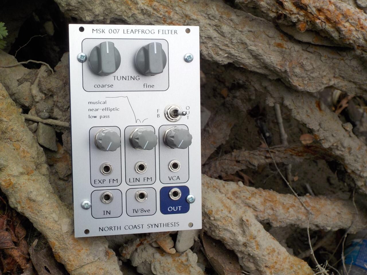
MSK 007 Leapfrog VCF
US$378.48 including shipping
Comments
Nice article, easy to understand, thanks! Now to go find out why the circuit I'm looking at is doing this!
Is your example from an old TL074?
However, also note that the text you quoted, from the top of the front page of the data sheet, says "VCC+". That's the positive rail. It pointedly does not mention the negative rail.
If you dig into the data tables later in the document, even in the very latest version on the TI Web site, you can see specifications for the common mode range which include the positive rail (as advertised) but do not include the negative rail. Not even in the TL074H redesigned chip.
The phase reversal issue is not symmetrical. Voltages near the positive rail keep the P-channel JFETs in their desired operating mode (reverse-biased junctions), so it's relatively easy for the chip to handle positive voltages, whereas voltages near the negative rail make the junctions forward-biased, and then the JFETs stop acting like JFETs. So you get phase reversal for inputs near the negative rail, and not near the positive rail.
In principle, if you had a different op amp with a similar general design but N-channel JFETs at the input instead, then the whole thing would be reversed, and it'd be positive voltages that would cause trouble. But I'm not sure there are any such op amps on the market today.