Build your own commercial module part 2: design and development
2023-11-30 design electronics byocm MSK 007
Once you have a clear idea of what commercial module you're trying to build, the design concept as described in the first part of this article series, you face the task of turning that concept into a design as such: an electronic circuit with all the details specified so that it can be manufactured on a commercial basis, with all the necessary side items like the layout of a printed circuit board, information on where to get all the parts, physical shapes of things like panels, and so on. This kind of design work is critically important to the success of the product, but it also demands a lot of technological skill, so it's often the stage where it makes sense to bring in a consultant to help.
With something electronic like a synthesizer module the critically important part is usually an electronic circuit and there's a tendency to equate "designing" the module with designing the circuit, specifically in the form of a schematic diagram. Really, there are other steps involved and even just designing the schematic is a multi-stage process. I like to break down the high-level steps as designing an initial circuit; development, which means working out the details and often refining aspects of the original concept; and physical design, including PCB layout, which covers building that circuit as a solid object you can touch.
Initial circuit: how will it work?
If you did a good job of defining your goal, then it will usually be clear right from the start what major sections the circuit will need to contain. It may make sense to draw a block diagram, or just make a list, or for a module with a simple function it may even make sense to just leave that implicit. Not much thought needs to go into the block diagram of a plain single VCA module; on the other hand, something with a less familiar function, like an octave switch, may be easier to understand and think about with a graphical description.
The above block diagram is from the MSK 008 user manual, and it illustrates an important distinction: it's focused on externally-visible function rather than the physical breakdown of the circuit. The module actually contains an important section called the "reference voltage generator" which supports the quantizer sections and is not shown in the above diagram. There is only one of it, shared between the two channels, so it isn't part of the per-channel block diagram. The reference voltage generator is clearly visible on the schematic, and is discussed in the circuit explanation section of the manual, but most users don't need to know it is there. When drawing a block diagram it's important to think about the purpose for which you're drawing it, and which parts need to be included or left out to best serve that purpose.
Whether the block diagram is drawn explicitly or left implicit, the stage where we think about breaking down the major functions into blocks is a good time to think about efficiencies. I recently had a consulting client show me a concept for module that would handle stereo signals. It needed to control levels, so the impulse would be to draw a triangle on the block diagram and label it "stereo VCA"; but with a little thought I was able to rearrange the functions so that the level control would be a single-channel (mono) VCA, saving a fair bit of circuit complexity. That kind of analysis can be done long before the stage of actually drawing a schematic.
Something else I like to do before drawing a schematic is count the chips. That is, the integrated circuits (ICs) that will be needed to build the circuit. With analog, that often means counting op amp channels. It's usually possible to make a good estimate of how many chips the design will need, even before you have a clear idea of which chips you want to use; and the sheer number of chips is a good indicator of other important variables like how wide the panel will need to be, how much circuit board space it will require (which bears on depth and overall physical design), manufacturing cost, and so on.
If I am planning to build a two-pole state variable filter, I can reasonably estimate that I will need two VCA channels, which will probably mean a single variable-amplifier chip like an LM13700 or 2164. I'll also need two integrators, which will be two op amp channels. If the variable amplifiers are linear current-controlled amplifiers like the LM13700 (not actually a VCA chip), then I'll need an exponential converter, which will mean at least one op amp for the "servo" and probably another for control voltage processing. If they're exponential voltage-controlled like the 2164 then I'll probably still need a CV processing op amp but (assuming the module itself will be exponentially-controlled) I won't need an exponential converter. So I'm looking at, bare minimum, two variable-amplifier channels and three or four op amp channels depending on whether I'll be building an exponential converter. Then I might think about throwing in additional op amps for input output buffering, or to do mixing to support special features like a notch filter output, and I have some idea of what each thing I add will cost in terms of chip count.
The chip count may reveal opportunities for introducing features relatively cheaply. For instance, if you really need one VCA and the chip you're going to use for that has two channels, then you are free to put in a second VCA somewhere else at low cost because you already needed that chip anyway. In the MSK 009 Coiler VCF, the unusual integrator design I wanted to use required additional op amps, so my first op amp count for the project came to seven units. Op amps come in packages of one, two, and four units, so it didn't make sense to use one of each of those and have three different chips just to make up the exact count. The sensible thing to do was put in two quad chips for a total of eight op amps, in which case I would have an extra op amp left over. I could have just not used the extra, but it meant I was free add an extra feature if I could do it with just one op amp. That ended up being the "rectifier" input, one of the things that makes the Coiler unique.
Once the overall function of the module is broken down into smaller pieces it's time to draw what I call an initial schematic - emphasizing that this is a starting point, but at the level of showing all the individual parts like resistors and capacitors in addition to the ICs. In the initial schematic the emphasis is more on what people call "topology" than on things like component values, because many of those will change during development. The topology is often more or less mechanical because each section may be a standard building-block type of circuit. The designer might say, "I want this section to be a Sallen-Key low pass filter, I want that section to be an inverting op amp mixer" and then they can just draw in the well-known topology for each of those things. Choosing component values is often a less mechanical process, but it's necessary to do at least a first cut of that for the initial circuit, even if many component values are likely to change during development.
Development: working out the details
I think of the initial circuit as complete when you have a schematic diagram that you may not have built yet, but you can build it and if it was competently designed, you can reasonably expect it to basically work. The initial circuit will do more or less what you planned for it to do when you wrote down your design concept. But that doesn't mean you have a finished design! From the initial circuit, there is still a lot of work left to do to turn it into a commercial product. It's important to budget both time and money for discovering and making the changes that will surely be needed.
Development mostly consists of building the thing, seeing how it works (or doesn't), and making changes to get it to be the best it can be. The first stages of this process could possibly mean "building" it in a circuit simulator rather than in physical reality, but you'll almost certainly also need to build a few real ones. There's usually a progression from less-realistic to more-realistic models and prototypes: after doing some simulation, maybe you build the circuit on a solderless breadboard, then on a stripboard, before making an etched PCB and something close to the final physical design. If you're careful with the scheduling, you can put off stuff like the final panel design and the sourcing of certain components until later in the process, so that those time-consuming steps run in parallel with development on other things.
I have listed "development" before "physical design" because I had to put them in some order, and development usually does start before physical design starts, but if you're going to build a module that actually goes into a rack to try it out then you need some sort of physical design for it, and you will need to do development on the physical design for things like panel layout. So there is really a lot of overlap between these two stages.
It can be valuable to get others to help you with development, whether you call that consultancy or "beta-testing" or something else. Be careful with bringing in others, however. Even if you don't pay your testers, you will at least have to supply them with prototypes, which cost money. Involving others in the development stage will certainly lengthen your timelines. You are likely to get "helpful" feedback on how you should scrap your design concept and build some other kind of module entirely, rather than on any specific questions you might have asked. Ideally, a professional developer (like a professional editor) should help you make your thing be the best possible version of itself, not change it to be something else.
Physical design: how it fits together
Physical design is probably the most underestimated step in designing a module, or any electronic product. Where does everything go? How big is everything and how does it all fit together? "Everything" in this case means not only solid components that might be listed on a Bill Of Materials, but also space, like the space around a knob so that the user's fingers can grab it, and the space between components on a circuit board where the copper traces will run to connect everything together. Physical design requires planning out the entire arrangement of physical objects and spaces that make up the product.
PCB (printed circuit board) design is one important part of physical design. Almost every manufactured electronic product uses an etched PCB, so you need to take the schematic and turn it into a layout for etching. The layout necessarily includes assumptions about the specific parts used. Whereas the schematic might just say "0.1µF capacitor," and the circuit would work electronically with almost any 0.1µF capactior, the layout needs to have two pads for the capacitor the right shape and distance apart for the physical object you're going to mount there. Not all 0.1µF capacitors are the same size and shape. So the PCB layout depends on sourcing the components, that is, deciding exactly which specific items you're going to use in your build, and that in turn depends on your plans for most of your manufacturing process. PCB layout as a result has to be closely connected with a lot of other decisions.
Work on the PCB design can feed back to the schematic through issues like gate swapping. I mentioned quad op amp chips above. If you have four op amps on the schematic, and four on the chip, and they're all identical, then which one is which? At some point, someone needs to decide that one op amp on the schematic will be the one on this corner of the chip, another will be that one, and so on. Ideally, that decision should be made so that the connections between the op amp chip and the other parts of the circuit will be laid out as neatly and compactly as possible; but this means the PCB designer needs a way to specify these decisions and have them fed back to changes on the schematic, where the information is recorded.
When there is more than one chip of the same type, then maybe the PCB designer should also be able to swap units between chips; but there can also be cases where two particular units on the schematic should not be on the same chip (to prevent them influencing each other), and that also needs to be taken into account. Avoiding undesired influence between different parts of the circuit also means that certain signal traces should not be routed next to each other, or even that it may be necessary to run extra traces in some places to act as shields. A good PCB designer needs to think about the magnetic fields created around all the traces or wires and how those will interact with each other, not only where the wires themselves go. I wrote about some of these issues in my earlier article on PCB design mistakes.
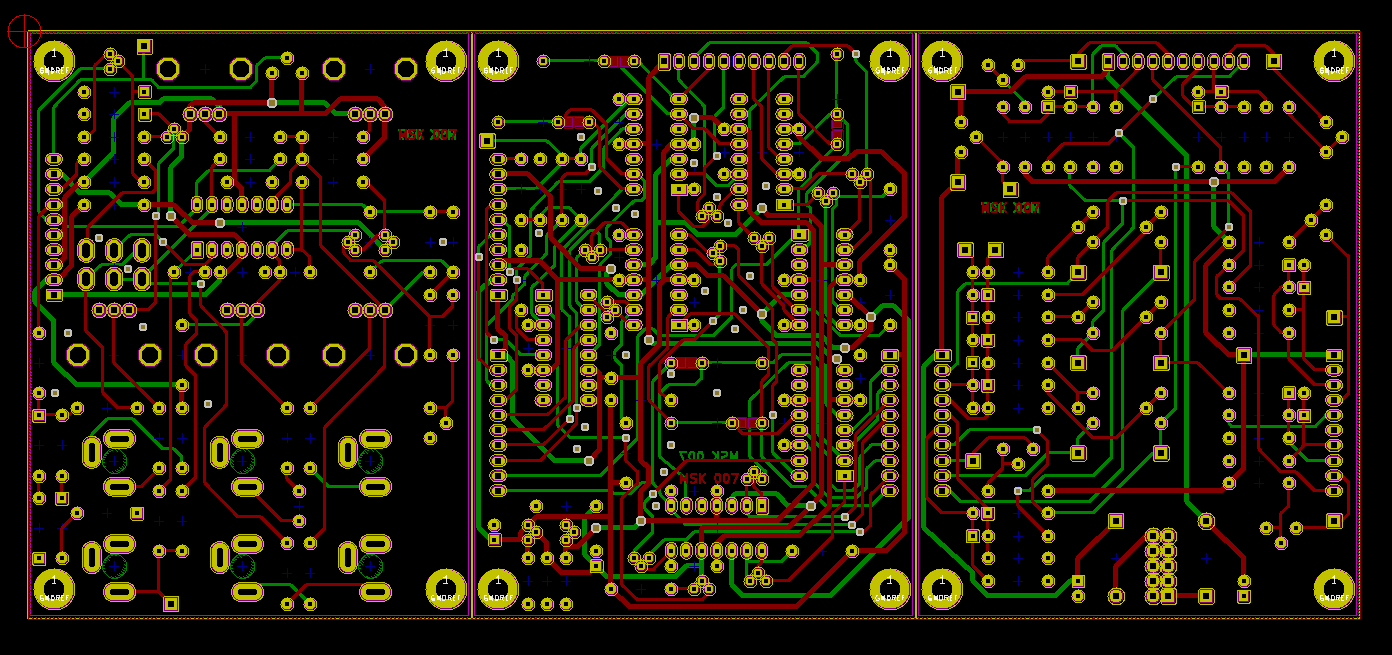
Laying out a PCB as compactly as possible while still respecting all the electronic and electromagnetic constraints on it is tricky, but because it is so difficult it is best done by humans. Even a beginner-level human designer can usually produce a better layout than auto-routing software would; automated PCB layout is still sometimes done commercially, but only where speed is more important than the quality of the result.
For a product that has controls and connections on a panel, there's quite often a PCB right behind the panel holding up the jack sockets, potentiometers, and so on. So the design of that PCB determines where all those things are in relation to each other, or vice versa. Locations of the controls and connections make up most of the panel design. If you're hiring a graphic designer to "do" your front panel, then that person will need to work closely with the PCB designer, and it's possible compromises between them may become necessary. It needs to be clear which things, if any, the front-panel designer is allowed to move, and then the PCB design needs to take those decisions into account.
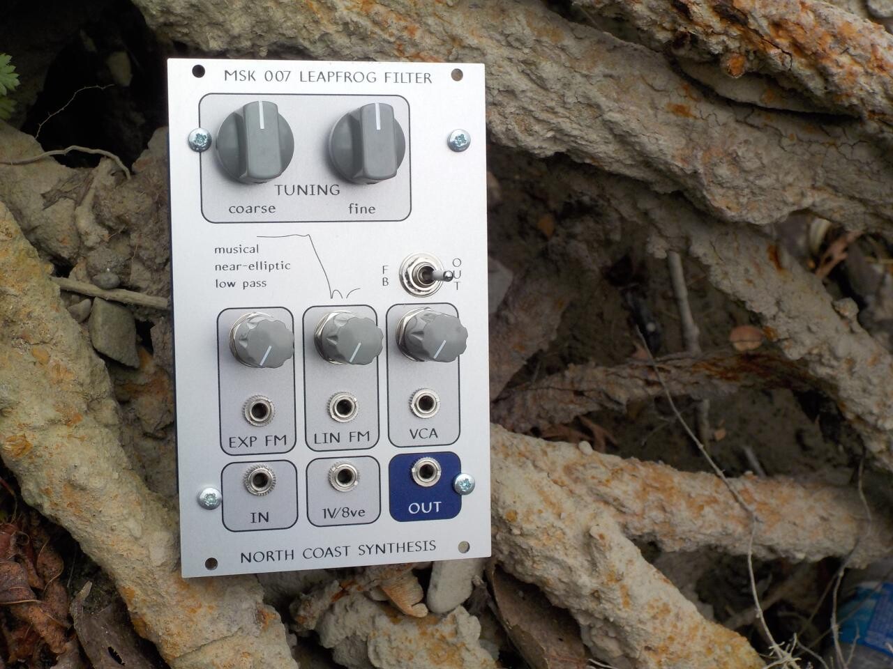
Other things may need to go on the behind-panel PCB besides the visible front-panel controls, including the bodies of potentiometers and encoders (often bulky, especially if they are high-quality units), connectors to other boards, and even significant parts of the circuitry. In North Coast modules I use bulky through-hole construction and often end up putting one or two chips of buffers and interface circuitry on the behind-panel PCB. That is only possible because I leave a relatively large amount of empty space on the front panels. With tighter-packed controls, many of my designs would overflow onto additional boards stacked up behind the panel. The MSK 007 Leapfrog is already a three-PCB module, and that's with the exponential converter on the behind-panel board (in the space between the tuning and modulation knobs). It would easily require four boards if I tried to close that gap, make the module narrower, and keep it through-hole. On the other hand, if I went to small-pitch surface mount and robotic assembly, I could probably drop one of those boards; but then it would be less suitable for DIY, and less repairable.
As well as the circuit board or boards, in a Eurorack module there will also be a front panel. Many DIYers and some commercial manufacturers get their PCB contractors to run off front panels on the PCB line, so they get fiberglass-laminated panels. That saves money, and perhaps more importantly, it's convenient, because they can use the same tools to design the panel that they're already using to design the PCBs, and have the same fast-turnaround small-volume manufacturing. It also means there's some possibility to build electronic functions (like those horrible "touch" keyboards) right into the front panel. But it also means limitations on how stiff and therefore how rugged the panel can be, and on the quality and variety of printed graphics available.
PCB panels also create pain points when the expectations for a PCB are different from the expectations for a panel. For instance, there may be limitations on what sizes and shapes of holes you can have made in a PCB, or on how the edges of the PCB will be finished. Most PCB contractors won't agree that a PCB is defective, and give you a refund for it, if it has cosmetic blemishes like scratches that make it unsuitable for a front panel but don't affect its electrical properties. From their point of view, they sold you a thing to make electrical connections, not a thing to look pretty as the face of a product. Maybe dealing with these pain points is worth it for the advantages of a PCB panel; if not, then you have sourcing questions regarding whatever you're going to use instead. Figuring out which tradeoffs you are willing to make on this kind of thing, is part of the physical-design process.
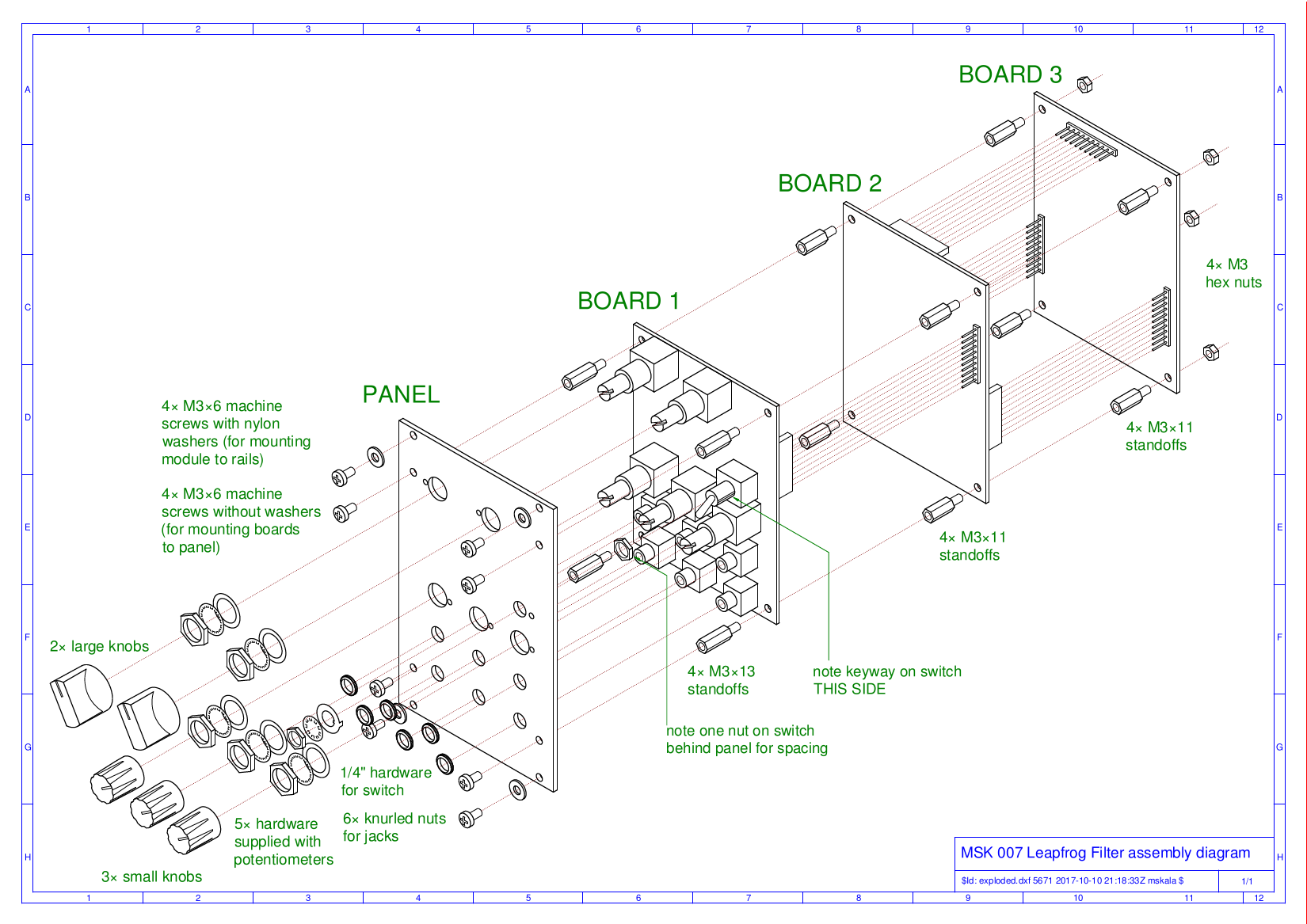
Given you have one or more PCBs and a panel, how will you physcially fasten them together? Will the potentiometers and jack sockets fasten with nuts to the panel, and then solder to the board behind, so that all the strain is transferred through the solder joints? If the jack sockets need a certain distance between the board and the panel, will the pots also fit into that distance? Will you use bushing-less pots, which do not fasten to the front panel but just poke through holes? Those cannot provide support to the board and they may feel "wobbly," but they allow for a smaller panel because they can be packed closer together, and that may be important. Will you have separate hardware for mechanical support, screwing into its own holes in the panel? I use separate hardware in most North Coast Synthesis modules, for strength and reliability, but the extra parts are quite expensive, and I've heard the claim that having visible screw heads is "low build quality" - which really made me wonder why I bothered. That's another decision to make as part of the physical design.
Although it may be more a matter of documentation than of design, I find it useful to prepare formal mechanical drawings of the physical design. At the very least, the exploded diagrams look pretty on the last page of each user/build manual; but these and the more functional 2D drawings also help me keep track of where everything else and how it fits together.
◀ PREV Build your own commercial module part 1: the design concept || Build your own commercial module part 3: firmware and documentation NEXT ▶