PCB design mistakes
2020-10-04 electronics design
Electronic design is sometimes imagined to begin and end with the schematic. Whoever drew the schematic gets the "designer" credit; hobbyists search the Web for "free schematics" and just assume they will encounter no issues getting from there to a working build; and technical documentation for modules (including my own) focuses on displaying and explaining a clear schematic rather than giving much or any coverage to the PCB design.
It's certainly true that the schematic is important, but laying out and debugging the PCB is also a very important part of designing a circuit. Let's go through some frequently-seen mistakes in PCB design. This is a kind of companion piece to my earlier article on design mistakes in synth schematics.
Here's a close-up of the power supply board from the first Eurorack case I owned. The manufacturer has subsequently changed the design, so they're no longer selling one that looks exactly like this.
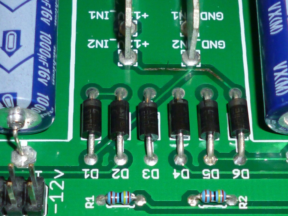
This board takes in low-voltage AC power from a wall transformer through the blade connectors in the upper portion of the photo, and rectifies it with the diodes in the lower portion. Despite the labels, the two blade connectors represent the two sides of a floating transformer secondary, not actually positive and ground. As seen in the photo, one of the AC traces has burned up. I'm not sure exactly how that happened. I think I may have shorted one of the outputs of the power supply briefly. But it illustrates a very common PCB design mistake: traces that are too thin.
Somewhere downstream from the parts in the photo is a typical three-terminal regulator with built-in short protection, so although the power supply was presumably overloaded, the burned trace can't have been very overloaded. The wall transformer was rated for 2A and the power supply was rated for 850mA output on each of the ±12V rails. So it's reasonable to expect that that trace would have been designed to pass at least 1A in normal operation, and it's reasonable to guess it might have been subjected to something like 3A when it was overloaded. It can't have been much more than that or something else would have tripped and shut off the power first.
From measuring the photo it appears that the burned trace is 10 mils, that is, 0.254mm. That's a pretty common default width for PCB traces in CAD software. There is no hard and fast law for how wide a trace has to be, because it all depends on how much you're willing to let it heat up. But there is a fairly well-agreed formula, specified by the industry group IPC and based on experimental data, for calculating how wide a trace needs to be to carry a given current given a choice for the acceptable rise in temperature. There are many online calculators for this formula; Digi-Key provides one.
Let's say that we are talking about a trace on the outside surface of a board (thus, exposed to air that could cool it; heat is more of a problem for traces buried inside multi-layer boards). It's "1 ounce" copper (usual default; see my PCB shopping article for more information on copper ounce thickness). The ambient temperature is 25°C (slightly above common room temperature, for inside a case) and we'll accept a 20°C rise in the temperature of the PCB trace for normal operation (which is plausible, though only 10°C might be a more common and conservative choice).
Under those assumptions, the Digi-Key calculator indicates that it's safe to run up to 1.2A through a 10-mil PCB trace. So if we're guesstimating that 1A is the maximum normal load, the trace should be okay for that - though without much safety margin. The calculator also says that to carry 3A (my estimate of what happened in the overload) it ought to be 35 mils. The IPC formula is not supposed to be used for temperature rise of more than 100°C, so we can't get a meaningful estimate of just how much temperature rise actually occurred, but 100°C temperature rise at 3A would correspond to a width of 13 mils, so we can say that with 10 mils it had at least 100°C of temperature rise, and that's certainly enough to cause some damage. It's a more than linear relationship, too; if my 3A estimate was a little low, then the real temperature could easily have gone high enough to burn off the solder mask and melt the trace as shown. The temperature rise for a 10-mil 1-ounce trace at 5A is outside the scope of the IPC formula, but would have been at least several hundred degrees.
So that's a PCB design lesson: when currents get over a few hundred mA, we have to actually do the calculation and make sure the traces are wide enough to carry not only the normal operating current, but also the amount of current that would reasonably be expected in a fault scenario.
The possibility of a PCB trace actually burning up from overcurrent is mostly something to think about with power traces, but too-narrow traces can also be a problem for signal connections. A 1-ounce copper trace 10 mils wide will have a resistance of about 0.02Ω/cm. It's easy for a trace in a synth module to be 10cm or 20cm long; then we're looking at a series resistance of 0.2Ω or 0.4Ω. Usually not enough to be a problem, but we certainly do sometimes have circuits in synthesizers with low enough impedance levels for that much extra resistance to make a difference to circuit operation.
Using narrow traces makes it easier to route the PCB because you can fit more traces into a given space, but most people make their traces too narrow by default. I think maybe it comes from looking at PCB fab specifications for the minimum trace width the fab can print, and taking that as a normal or expected value instead of an extreme. As well as creating current-handling and series resistance problems, narrow traces are harder to manufacture and so they increase the cost of making the boards - better process control needed to prevent them getting etched away, better quality control needed to detect that kind of defect when it does happen.
Some boards do need very high density and narrow traces as part of achieving it, especially when dealing with machine-assembled narrow-pitch surface-mount components; but through-hole boards for hand assembly in particular usually don't need the traces so narrow as 10 mils. And if there's space to do it, it doesn't cost any more money to use wider traces. My usual guideline for through-hole trace width is 20 mils for signal traces and 35 mils for power. I would only shrink traces smaller than that if absolutely necessary, after careful exploration of other alternatives.
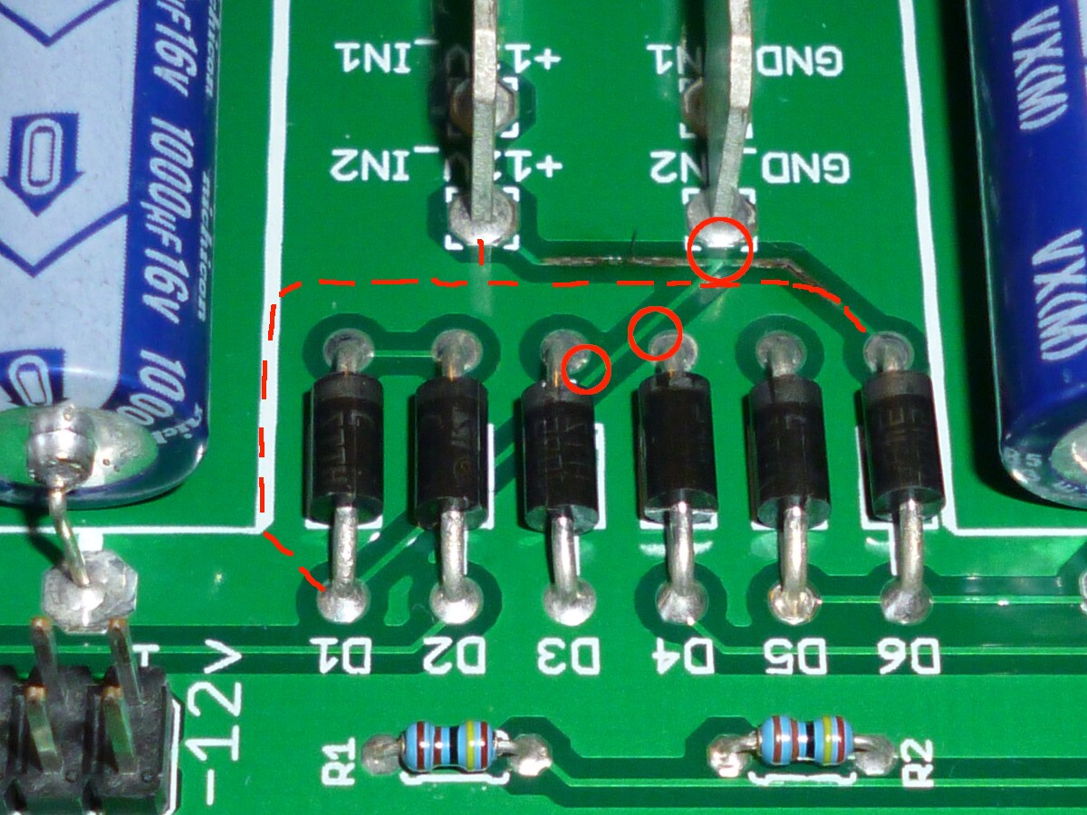
Something else is worth noting on this board: the routing of the trace that burned up isn't the best. One branch of that trace goes diagonally between two of the pads for neighbouring diodes, and then cuts very close to the other blade connector, with close calls at the points shown by the red circles.
Now, the trace is insulated by the solder mask (and even without that, the air alone would be a good insulator), so it can actually come quite close to another voltage without there necessarily being an interference problem. The voltages here are low; there won't be any high-voltage sparks jumping across those gaps. PCB designers usually run an automated "design rule check" (DRC) before shipping out a board design, minimum gap size between copper at different voltages is one of the main things the DRC looks for, and it's likely that this design would pass such a check.
However, just as with trace width, the minimum gap allowed between two different nets in a DRC will usually be the minimum that could be acceptable, not the minimum that is really advisable. Remember the "pieces of flair" in Office Space (YouTube link): Stan may be an asshole, but he is not actually wrong. Just doing exactly the bare minimum doesn't encourage confidence that you are really doing your best. Even after passing DRC there's still some responsibility placed on the human beings, and it's better to have wider gaps than minimum where possible.
Narrow separation between different nets makes the PCB manufacturing that much harder, and also creates greater sensitivity to defects, assembly problems, and so on. For instance, when hand-soldering a through-hole pad it's easy to scratch through the solder mask near the pad, and then if there's a trace there, it's easy to short it to the pad with a bit of stray solder. I had one batch of boards where the solder mask was slightly misaligned, creating a pinhole to the exposed ground plane near each pad, and it resulted in a bunch of pins on header connectors getting shorted to the ground plane when I assembled the boards. Keeping wider separation, and avoiding running traces between closely-spaced pads, makes such problems less likely and is better general style.
Sometimes a close call of a trace near a pad is necessary, but in the photo, the close calls seem unnecessary. Unless there's some other important consideration I'm missing, it seems that that trace could easily have been run along the general path I've drawn in with dashes instead. It could have kept a much greater distance from both the diodes and the blade connector instead of nearly clipping their pads. Going around the side would make it a couple centimetres longer, but the designer clearly didn't think resistance was a big problem anyway, else they would have used a wider trace to begin with.
If for some reason it was really necessary to run that trace between the pads of D3 and D4 instead of going around the side, then instead of running it diagonally, it should have been possible to add a corner and run the trace vertically through the gap, significantly increasing the separation between the trace and the pads.
One specific case of running a trace between nearby pads comes up a lot, and that is routing traces between adjacent legs of a DIP IC. I'm not going to say "never do that." My 20-mil signal trace guideline is partly chosen so that I will (just barely) have space to route such traces between DIP pads when I want to, bearing in mind the minimum separation and "annular ring" design rules that I also use. I have a high-density digital design I'm working on right now where I am running traces between DIP pads in a few places. In that design in particular, I'm using a long skinny 28-pin DIP microcontroller, so there are 1.4-inch rows of pins on either side that would be complete barriers to routing if I allowed no traces in between. Following it as an absolute rule in this case would necessitate some very long detours for high-frequency signals (leading to EMI problems), a routing crunch near the ends of the DIP, and so on. Allowing a few traces between the pads is a worthwhile compromise. But on less demanding boards, I try pretty hard to avoid it. And I often see it happening for what seems to be no reason at all on boards that seem not to have been carefully designed.
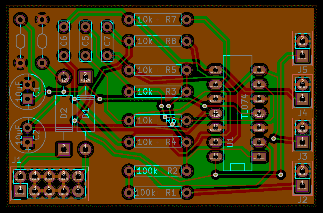
Here's a made-up example of the kind of board design often seen in synth DIY. This board passes DRC; you could get it made up and assemble the components on it and it would work, probably. I've seen plenty of board designs that look like this being sold in the DIY market. But this is not a good board design and it shouldn't be considered professional standard.
The view shown here is a screenshot from KiCAD with the settings I usually use while editing boards; it's assumed that there is a ground plane on both sides, but display of that is turned off, in order to make the other connections easier to see. More on that later.
First off, there are a bunch of traces on this board routed between the pads of the DIP. It might take some work to eliminate all of those, but some of them would be easy to remove. For instance, the trace from pin 8 of U1 to J4 could easily go up and around instead of threading between the DIP pads. There's plenty of space for it above the DIP, and doing that would relieve some of the space crunch under the DIP, making room for other improvements.
Several other problems are visible in this design. The traces are all too thin (I let them default to 10 mils), and there's basically nowhere on this board that that provides an advantage. Many of the traces are at funny angles instead of the 45° increments enforced by most CAD software. Some people think that looks cool, because it resembles the style of old-fashioned hand-painted PCB designs from before the computer era. But it's much harder to properly control the spacing of traces when they go at funny angles. Close calls between traces, like the ones on the burned power trace in my earlier photo, become much more common as soon as traces are at funny angles. This example board actually does pass DRC, but getting it to pass DRC becomes a struggle with traces not at 45° multiples - and the traces also tend to hit more points on a square grid, making routing in general much more difficult. It's better to avoid these issues by sticking to the conventional angles.
Take a look at the cluster of vias around the power diodes at the left. These are places where a trace has to pass through the board to the other side: there's a little hole drilled and plated through, and the trace runs up to it on one surface of the board, makes a connection through the hole plating, and then continues on the other surface. Vias are often useful, but having too many of them can be a problem because they take up space, complicate the EMI picture, and may increase the cost of making the board. In this particular case, if the trace from R4 to C6 were on the top (red) all the way instead of dipping to the bottom halfway through, then we could also drop the 12V trace from D1 to C1 onto the bottom surface, and eliminate a total of three vias. Similar small, but interacting, changes elsewhere could probably eliminate most of the other vias on the board.
It's a common pattern when people use auto-routing that the auto-router will end up putting in unnecessary vias. From a computer science perspective, routing PCBs is a very difficult problem (NP-hard or worse), and it's the kind of task that human beings tend to do better than computers can. It's difficult for computers because of the interaction among traces: if you want to move one trace to the other surface of the board, then you may also need to move several others to make room for it, and there can be arbitrarily complicated logical relationships between them. Even a beginner-level human designer can usually think through these issues to produce a tighter, better PCB design than what comes from auto-routing software. The best auto-routing software is terribly expensive and still doesn't work very well. The reason auto-routers are used at all is in cases where there's a serious crunch for time or money and someone decides they can't afford human effort on the project. But even if it seems necessary to apply auto-routing to a board, you can often get a better result by spending a little bit of human effort on it afterward to clean up points like these unnecessary vias, and the traces between DIP pads mentioned earlier.
Here's the schematic for my example board. It's meant to be what in modular synthesis is called a "buffered multiple" (those in other fields of electronics might call it a "distribution amplifier"). At lower left, you can see the power decoupling: two 10µF electrolytic capacitors intended to absorb some of the garbage that might be present on the incoming power supply, and two 0.1µF decoupling capacitors associated with the DIP IC.
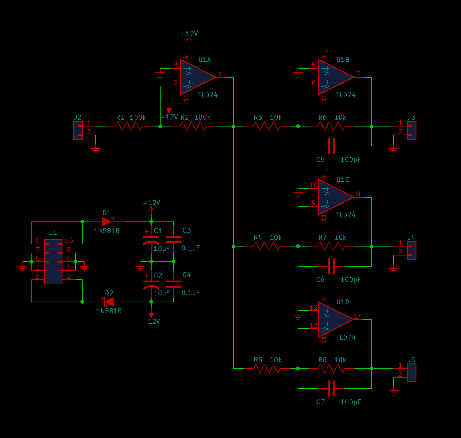
I usually prefer to draw decoupling capacitors on the schematic right at the points where I show the power connections for the IC in question (so, next to U1A in this example). But grouping them all together off to the side is also a common practice; people do that in an effort to make the schematic easier to read. The problem is that although it doesn't matter on the schematic where the capacitors may be located, it does matter on the board. Take a look at the board design again.
The decoupling capacitors serving the IC are off in the upper left corner, far away from the IC. The point of having these capacitors is that if there's a sudden spike in the IC's current demand, it can draw energy from the decoupling capacitors instead of needing to wait for it to arrive along the power lines. An equivalent description is that the decoupling capacitors provide a low-impedance shortcut for high frequencies between the power pins of the chip.
But in this design, the "decoupling" capacitors are so far away from the IC's power pins that they won't be able to help as much as they should. Current spikes from the IC will have to contend with the resistance and inductance of those long traces before getting to the capacitors. At very high frequencies, the traces on the board present a high impedance in series with the capacitors, eliminating the low-impedance shortcut.
Putting decoupling capacitors far away from the chips they support is a common error for people working from schematics they've downloaded from the Net. Someone who doesn't understand the purpose the decoupling capacitors serve may be inclined to see a capacitor on the schematic, put that capacitor on the board, and say "Done!" It also gives rise to the question we sometimes hear from more advanced hobbyists: if the schematic shows five or six small capacitors in parallel, "Why not just combine those into a single bigger capacitor?" Why not, indeed? As I've discussed before, multiple pure capacitances can be simplified into single components. The answer is that there are other considerations, which the schematic designer may not have spelled out clearly, regarding the way the PCB ought to be laid out.
A well-managed workflow will not just consist of designing a schematic and then designing a board to match it. Information can flow in the other direction, too. Quite often, there will be points discovered during the board design that inform necessary changes to the schematic. One of the most common is gate swapping.
The TL074 quad op amp contains four identical operational amplifiers. They're labelled with letters: U1A is the unit connected to pins 1, 2, and 3 of the chip; U1B is the one connected to pins 5, 6, and 7; and so on. The schematic shows which op amp unit is connected to which other parts of the circuit: unit A handles the input, and each of the others drives one of the outputs.
But the assignment of op amp units to different parts of the circuit is arbitrary, as far as the schematic is concerned. There's no reason that unit A needs to be the one that serves the input. It might be that some other assignment would make for a better PCB layout. In particular, look at J5; it is connected to pin 14 of U1, because the schematic says that unit D is the op amp unit for J5. That's the most distant pin on the chip from J5. It would make a lot of sense to swap units B and D; then the trace to J5 could cover the much shorter distance from pin 7, and by removing that long trace, other parts of the board could be simplified, too. So ideally, the PCB designer would be given the option of redefining which unit on the op amp chip serves which function. Then that "gate swap" decision would propagate back (possibly by means of an ECO - an "engineering change order" in larger organizations) to a change in the schematic.
In a more complicated circuit with multiple chips, there may even be some gate-swapping across different chips; but there can also be reasons not to do that, related for instance to crosstalk. At one point in the Middle Path VCO design I ended up splitting a quad op amp chip into two dual op amps, because I didn't want op amps from the two oscillator cores to be on the same shared chip where they might possibly interact. Splitting the chip also meant I was able to keep several other parts of those oscillators far apart on the PCB. These issues make PCB design more interesting and complicated than just an exercise of routing lines around on the screen; the PCB designer ultimately needs to know about all the electronic considerations that went into the schematic.
I've left to last what may be the most controversial PCB design mistake on my list: the question of ground planes, or perhaps more correctly ground pours. The CAD software used for creating board designs can be directed to fill all parts of the board that are not otherwise used, with copper connected to the ground (0V) voltage. Then components that are meant to connect to ground don't need explicitly-defined connections. They will just automatically tie into the nearest point on the ground pour. As I mentioned, I usually have my KiCAD installation set up to hide the ground pour, for better legibility of the screen display, but when it is set to display explicitly, it looks like this.
Ground pour means that the computer will automatically fill in the spaces between and around PCB traces with extra copper, and connect everything that should be at 0V ("ground") to that copper. It's called a "pour" because the copper is imagined to flow across the board, into all the nooks and crannies. It doesn't go absolutely everywhere because there may be some areas boxed-in by traces, with nothing inside connected to ground; but it usually covers most of the surface. The main consequence of ground pour is that there is a low-impedance, and especially low-inductance, path between any two points that are supposed to be at 0V.
The ground pour functions as a very wide trace itself, usually with better electrical properties than you would get by explicitly drawing in an ordinary trace to make the 0V connection. It also serves to shield electromagnetic interference (EMI) because any radiation from signal traces will tend to be captured and blocked by the extra copper. There will be a certain amount of stray capacitance from every trace through the board to the ground pour on the other side, which can serve as both decoupling and to enhance stability. In general, ground pour kills the circuit's response to very high and ultra-high frequencies (hundreds to thousands of MHz). In audio circuits, you don't want the circuit to do anything at those frequencies and a PCB feature that tends to eat them is beneficial.
I am mostly interested in two-layer boards, with ground pour on each side. I normally route signals on both sides of such a board, let the ground pour fill in the empty space on both sides, and call that good enough. In higher-density and higher-frequency boards with more than two layers, it's a fairly common practice to designate one (sometimes even more than one) entire layer to carry only ground, with the signals on the remaining layers. Then the layer designated as a solid ground becomes a "ground plane." But that's more relevant at higher frequencies than audio, where the advantages of having a uninterrupted ground plane across the entire board are more significant.
There may be an environmental advantage to manufacturing boards with ground pour, because PCBs are manufactured by what might be called subtractive synthesis: the fab starts with a board covered in solid copper foil and then uses chemicals to etch away the parts that are not meant to be copper. The copper that gets removed does eventually get recovered by re-refining the etching liquid (it's too valuable to just put it down the drain), but leaving more copper on the board means less expenditure of chemicals to remove it, and probably a net win for the environment.
I think that in general, and especially for audio circuits, you always ought to use ground pours by default, unless you have a specific and well-informed reason not to do so on a particular project. If you are unsure, you are more likely to get into trouble by not using a ground pour, than by using one. When I see a board without it, I usually think that's not a well-designed board. I expect to draw some flames for saying that.
Some of the objections to ground pours come from taking a negative view of the features I see as advantages. In particular, using a ground pour means there will be stray capacitance between each trace and the ground on the other side of the board. If the frequency is high enough, and if the traces are long enough, then that stray capacitance can add up to enough to affect circuit operation. Amplifiers can become unstable with too much stray capacitance at their inputs. A trace drawn across a board with a ground pour on the other side, at high enough frequencies, is no longer a theoretical wire; it becomes a transmission line, with a characteristic impedance of its own. Signals can travel along such a line, bounce off the impedance mismatch at the other end, set up standing waves, and generally misbehave.
But these effects show up at frequencies in the hundreds to thousands of MHz. They are not relevant at audio. All too often I see people posting well-actually stories on Web fora purporting to "explain" that ground pours are a bad idea, citing scientific articles... that are full of graphs with the axes labelled in GHz! By all means if you are dealing with radio frequencies where the transmission line effects are significant, you need to design your PCBs accordingly. But even then you often do end up wanting to use a ground plane (with carefully controlled trace width and dielectric constants, turning your traces into "microstriplines"). It's possible that an inadvertently created microstripline could act like an antenna and transmit or receive interference - but it's much more likely that a plain trace without a ground pour on the other side would do that. And these considerations are seldom relevant at audio.
Another objection to ground pours is in the opposite direction, saying that people will rely on them too much. You get some stray capacitance from every trace to ground, and that can help with stability and decoupling, but it's usually not enough that you can leave out deliberately-installed capacitors. You get some radiation shielding from the ground pour but maybe not enough to excuse other practices that are questionable. You can't just design a board with a ground pour and leave out the decoupling capacitors; the capacitance resulting from the ground pour is nowhere near enough to be a substitute. (Except in certain specialized boards where entire layers are designed to provide "embedded capacitance" in a controlled way, but that's not the normal case.) You can't just ignore possible electromagnetic interference and depend on the ground pour to prevent it. I'd say that it still makes sense to use the ground pour because it will likely reduce, even if not always eliminate, these issues.
Finally, I've heard an objection to ground pours related to the matter of disconnected copper islands. Depending on the design of the board, it's possible for the signal traces on a surface to box in an area where there actually are no ground connections. A copper pour in that area will not be connected to ground, nor to anything else, and that's said to be a problem. (The usual line is that it will "pick up noise.") There are a couple of such islands in my example board; they're not easy to spot in the complete view showing all the copper, but here's a stripped-down image highlighting them. Note how the solid copper areas in the centre do not actually connect to any component pads. They're completely surrounded by traces, with gaps too narrow for the copper pour of the island to escape and connect to the grounded copper around the outside of the board.
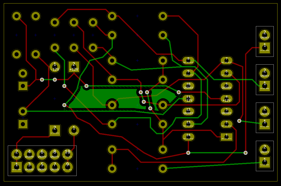
Isolated islands are claimed to be a big problem and a reason not to use ground pours at all. But they are not actually a real thing! Present-day CAD software when used in the normal way does not create them. It will automatically remove the copper from isolated areas. In order to get that isolated island onto my example board, I had to manually draw it in - KiCAD refused. Maybe in the old days when people were creating PCB art with felt pens and paint brushes, it would have been easy to do this by accident and it would make sense to warn them to make sure all parts of the pour really connect. But even then, it would be a reason to be careful, not a reason to avoid ground pours entirely just in case.
The claimed problems with isolated islands of copper are a little iffy anyway. I cringe every time I see a claim that unconnected things (copper islands, traces, wires, unused jack sockets, and so on) will "pick up noise" through radiation; people really seem to think that that happens routinely and is a major design consideration for audio circuits. With a few narrow exceptions (such as the ferrite rod antennas used for AM broadcast receivers), any antenna absorbs radiation with wavelength on the same order of magnitude as the size of the antenna. An object 2cm in size is only going to receive radio signals with a wavelength of at most about 8cm, which means a frequency of at least about 3.5GHz. That means you have to think seriously about this kind of PCB feature acting as an antenna when you are building something like a cell phone, which really operates in that frequency range... but not at audio.
A more legitimate reason to be concerned about isolated copper pour islands would have to do with capacitive coupling: you could have a trace that crosses the island on the other surface of the board, signal from that trace gets coupled into the island, then coupled from there to another similar trace. If the island were properly grounded, the coupled interference signal would be diverted into the 0V; but with the island floating, it can be a way for signals to couple between things that should not connect. So, yes, isolated islands would be a problem in that way, if they existed, which they don't, because the software doesn't create them.
Because the software will remove copper from areas that would be isolated, there can sometimes be significant areas left open without a ground pour, and those areas don't get the benefit. Even when it's technically possible for the ground pour to connect, it may be that there are so many traces cutting it up that the actual path for currents through the pour is long and convoluted, passing through narrow gaps that increase the impedance. If a signal trace on one surface has to cross a slot in the ground pour on the other surface (such as might be created by another signal trace on the opposite side), then the return current for that signal has to detour around the slot. Such detours maximize whatever electromagnetic interference problems may occur, even if they are not usually a big problem for audio. And if there are ground pours on both sides of the board only connected to each other in a few places where a through-hole component hits both, then there can be similar detour problems when a return current needs to pass through the board from one surface to the other.
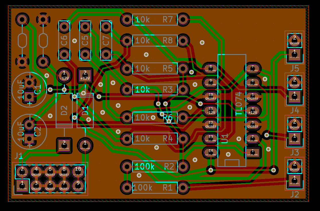
So it's good practice, when designing a two-sided board with ground pours on both sides, to add some extra vias connecting the pours on the two sides. An area on one surface that is isolated (and so the copper would be removed by the software) will usually be at least partially covered by a pour on the other surface; adding a via at that point allows the software to fill the area with a non-isolated copper island. Adding more vias in board spaces that are covered by both pours, allows ground currents to take shorter and less complicated paths. Manufacturing considerations may limit how many extra vias the PCB can support (in some cases, they may cost money), but if it's easy to add them, it's usually worthwhile to add extras. High-frequency boards where the electromagnetic considerations are more significant use this technique in a more formal way, such as with rows of vias at a specified interval bracketing either side of a microstripline to make sure the return currents flow exactly as planned.
Here's my example board with extra vias added. Note that the islands I highlighted earlier are now properly connected to the surrounding ground pour, by going through the pour on the other board surface.
To conclude, I've gone through some issues I frequently see in synth DIY boards: traces too thin; close calls in routing; traces between DIP pads in particular; traces at funny angles; traces that bounce between the surfaces of the board too much; the limitations of auto-routing; decoupling capacitors too far away from the chips they serve; lack of gate swapping; and ground pour issues. Many of these are best understood as trade-offs rather than as firm rules: often it ends up being worthwhile to break one of them in order to be able to do better on another point. But all these points are worth knowing about.
◀ PREV Genome Jazz || Vexations NEXT ▶