Transistors for the Perplexed
2018-07-08 electronics design
Most transistor circuits are quite straightforward. If you look at the schematic of something like the North Coast Transistor Mixer, you can easily recognize common patterns - an emitter follower here, a common-emitter amplifier there - which are in every textbook and really are just transistorized versions of vacuum-tube circuits going back generations. The new Transistor ADSR gets a little more complicated, largely because of its use of two-transistor circuit blocks such as multivibrators, but there's still nothing really weird in it. But every now and again you'll see something in a schematic diagram that isn't in the textbook, seems like it makes no sense... and yet, it works. This article covers a couple of those non-traditional ways to use transistors - as well as some simple, obvious questions that smart beginners are likely to wonder about but which aren't usually answered in introductory presentations.
An upside-down transistor
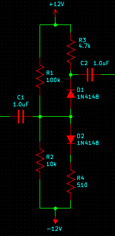
Analog percussion synthesizers often contain something like the following.
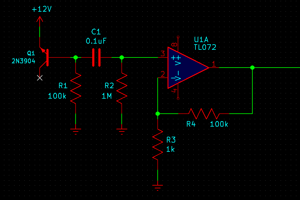
What is going on in that circuit?
The capacitor and everything to the right of it form a straightforward AC-coupled amplifier with a voltage gain of 100. (Note the DC bias resistor R2; leaving that out in AC-coupled op amp circuits is a common mistake and can have confusing effects.) Okay, so this is boosting a weak signal. But the components at the amplifier input, Q1 and R1, don't make much sense. From the context it seems like they are generating the signal that the amplifier amplifies. But the transistor is upside-down, with its base-emitter junction reverse biased and its collector not even connected at all. Output is being drawn from the base, which is normally the input of any transistor circuit. What's up?
In fact this, is meant to be a noise generator circuit. As specified on the 2N3904 data sheet, the base-emitter junction of the transistor is rated for an absolute maximum reverse voltage in normal operation of 6.0V. In practice, individual examples may be able to withstand a little more, like 7 or 8V, but not the 12V being applied here. The junction will undergo some combination of Zener and avalanche breakdown (probably more avalanche than Zener at this voltage) and allow reverse current to flow. The resistor R1 limits that current to a level that will not completely destroy the device - although the process is still sufficiently destructive that a transistor used this way may no longer operate within its specified parameters when used as a normal transistor.
The reverse current through a PN junction in avalanche breakdown is noisy. Each time an electron overcomes the energy barrier involved in going backwards through the junction, it lowers the barrier for several others (hence the name "avalanche"), creating a tiny pulse of current; and there are many billions of these pulses per second, with random timing, creating noise with a well-behaved spectrum far into the gigahertz range. The current is still very small, though, and the amount of noise in the current smaller yet, so a fair bit of amplification is needed to bring it to useful levels.
Why use a transistor for this and not an avalanche or Zener diode as such? Indeed, many people do build this kind of circuit with a diode as the noise source. I think one reason for using a transistor may have to do with history: semiconductors in general were once much harder to come by than they are today (though discrete semiconductors are starting to become hard to find again as the world moves to ICs), and it may have been easier to just use another common 2N3904, which you would already have in stock, than try to source another part number just for a noise-generating diode.
Some people claim that one type of device or another produces noise that sounds better, or better levels of noise. Since avalanche diodes sold as such are more often used for tasks like voltage regulation, it's usually preferred for them to produce as little noise as possible, and manufacturers can be expected to optimize for that; the transistor junction, which is not meant to be run in reverse at all, won't be optimized for low noise in breakdown mode and might be expected to give better levels in this exotic application. On the other hand, precisely because it's not the intended use of the transistor, individual examples of transistors (even the same model) may be inconsistent in the amount and character of their noise output. Some people go to lengths to test individual transistors and pick out the best one for noise generation - though since testing them in this circuit ruins them for other purposes, it's a practice that entails some waste.
Since the noise level varies per transistor, it may not always be satisfactory to use a fixed-gain amplifier such as I've drawn. The output may end up too low or too high (driving the amplifier into clipping and ruining the spectrum). If you want to really build the circuit, you may need to put in some kind of at least manual gain adjustment; trying to do automatic gain control is possible but usually ends up distorting the spectrum again. Really, if you need consistent noise levels in a production environment where you will be building the circuit many times over and can't mess around with swapping in different transistors, you have a good application for a digital noise generator.
Why not use the collector-base junction instead of the base-emitter junction? You could. However, the collector-base junction is usually rated for a much higher voltage (40V in the case of 2N3904), so it's usually inconvenient to force it into breakdown. Also, since a high breakdown voltage on that junction is desirable for transistors in normal use (whereas for the base-emitter junction, it normally only needs to be high enough, and is traded off against other parameters), it may be even harder to guess what the real breakdown voltage as opposed to the guaranteed minimum, really is for the collector-base junction.
Two diodes = transistor?
The traditional diagram of a semiconductor junction diode looks like this. I don't know why the semiconductors in these diagrams are always drawn with rounded-corner rectangles, but never mind, it's traditional.
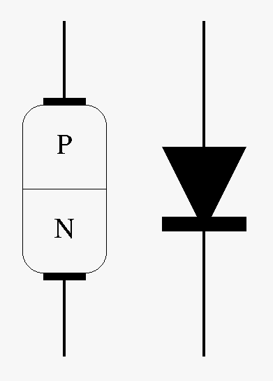
Anywhere you've got N-doped semiconductor in contact with P-doped semiconductor, in principle you have a diode. In fact they don't even need to both be semiconductors; the really old point-contact or hot-carrier diodes, used in crystal radios, consisted of just a sharp metal point in contact with a semiconductor surface, a fact echoed in the schematic symbol for a diode at right in the diagram. Schottky diodes, which I use for power supply reversal protection because of their lower forward voltage, operate on a similar principle.
But the classic junction diode is just formed anywhere two differently-doped semiconductor regions are next to each other. A junction transistor contains two such junctions back to back; and we've already seen that they can actually be used as diodes. So isn't a transistor really the same thing as two back-to-back diodes?
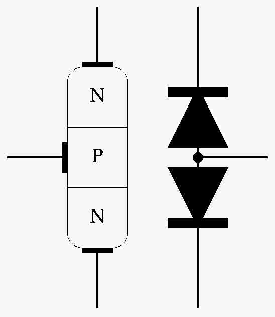
It seems like we ought to be able to build a transistor amplifier using two diodes, without a transistor. And this might be better because it means we can choose the two diodes independently, maybe allowing the creation of a wider range of transistor parameters. Why do we need transistors as such, at all?
But if you actually build that, it won't work. Why not?
The answer is it makes a real difference that the backsides of the two diodes in a transistor are fused together and not connected by a wire. What the traditional round-corners diagram maybe doesn't make clear is that the "base" region of the transistor, the P-doped region in an NPN transistor, is really thin - so thin that the two PN junctions can interact with each other in a way they couldn't if they were separated by a wire. It is also important that the base region is not a metal wire; it is a semiconductor.
Current in a wire is carried by electrons, which flow in the opposite direction from the abstraction of "conventional current" used in analysis. But the current in a semiconductor is really two currents flowing in opposite directions at once: one of electrons, and one of "holes," which represent places in the crystal lattice where there would normally be an electron, but one isn't there right now. Having these two currents at once creates the possibility for effects that would not happen with current flowing in a wire.
Remember that when a transistor is used normally, the collector-base junction is reverse biased. Normally, reverse-biased diodes (that are not breaking down) do not pass current at all. Yet a transistor in normal operation does pass current. It is by virtue of the interaction with the base-emitter junction that that can happen: current through the forward-biased base-emitter junction creates a population of electrons and holes in the base region, which disrupts the barrier at the collector-base junction, allowing current through despite the reverse bias.
To use one of the terrible analogies people are so fond of when explaining transistors, consider a crowded highway where a small but important minority of drivers want to exit on a certain ramp. If the ramp is heavily crowded, those drivers waiting for it will hold up traffic on the main highway and everything will slow to a crawl. That's like a transistor in amplification mode: the potentially large current through the collector is at the mercy of the electrons exiting (conventional current flowing in) through the base connection. But if instead the entire highway were diverted into a city, with traffic flowing through many different city streets with plenty of capacity, and then there were another highway on the other side without a direct connection to the first... that would be like trying to build a transistor with back to back diodes connected by a wire. Overall flow from one highway to the other would not be dependent on a small minority of cars leaving the city by some other route.
Another upside-down transistor
Another thing it's easy to notice in the traditional round-corners diagram is that the transistor looks symmetrical. Just looking at the diagram you can't even tell which end is supposed to be the "emitter" and which end is supposed to be the "collector." You have to infer that from the biasing. So why not swap them?
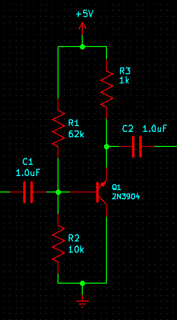
The two PN junctions in the transistor clearly are different from each other, because they have different breakdown voltages. But they both are PN junctions. Nothing in the usual description of how a transistor works mentions anything special about one junction that makes it different from the other and could prevent them from being swapped. I've said it matters that they have their backsides fused together instead of connected by a wire, but that is still the case in this circuit. So why can't we do this?
In fact, we can do this. It's sometimes called the "reverse active mode" of transistor operation. I haven't built the specific circuit above - the component values are guesses at what would make sense - but in principle it should work, and other circuits using transistors in this way do work.
One big drawback to the reverse active mode is that because the base-emitter junction is being reverse biased, voltage is limited to what it can handle. That's why I drew the circuit above as having just a +5V power supply; the 24V (+-12V split) supply used in Eurorack would blow out the transistor, pushing it into avalanche breakdown like the noise generator at the start of this article. Another drawback is that the gain of transistors in reverse active mode is usually very low, and (like other transistor parameters not used in normal operation) unpredictable.
At one point I played around with a transistor VCA design built on a reverse-active-mode transistor. I never made a complete module out of it, though, and I probably won't. It didn't seem like it would have any real advantage over other designs except being a cool concept - there's no reason to think it would sound better or interestingly different from other designs - and it doesn't look to me like people are willing to pay for a handmade module just to know that the circuit design is unusual.
Why is the base-emitter breakdown voltage so low?
Because the emitter is heavily doped; and that, in turn, is because the emitter ought to be more heavily doped than the base in order for the transistor to have a useful amount of gain. We want the current through the base (which is due to holes injected at the "ohmic contact" where a metal bonding wire is connected to the base region) to be a lot smaller than the current through the emitter (due to electrons injected at the emitter's ohmic contact). The ratio of these things is a big part of what determines the gain of the transistor; so for high gain, we need heavy doping at the emitter. And having one side of the junction be heavily doped also has the effect of reducing the breakdown voltage, because the effects that trigger breakdown are related to things that happen around the dopant atoms. More of those, and breakdown is easier.
Thus there's a tradeoff between high gain and low base-emitter breakdown voltage, and we should expect that higher-gain transistors will have lower breakdown voltages. In fact, if you look at data sheets of different transistors, the expectation is correct. The 2N3904 general-purpose NPN transistors mentioned above, for instance, are rated for 6.0V of base-emitter breakdown voltage and minimum current gain variable with overall current but peaking at 100. (I use minimum current gain because it's specified more thoroughly than maximum or typical values on this data sheet.) Compare those with 2N5088 transistors like one ones I used in my recent Transistor ADSR design: they are rated for minimum gain of 350 at the current where minimum gain is maximized, but the breakdown voltage of the emitter-base junction is only rated for 3.0V. Those transistors are optimized for higher gain than the 2N3904 type, at the cost of being more sensitive to reverse voltage.
In the other junction, between the collector and base, there is not this requirement for heavy doping to increase gain. So the collector is usually much less heavily doped than the emitter, allowing that junction to have a higher reverse voltage. This is a big part of the reason gain in "reverse active mode" is usually low.
Here's a clip from the Transistor ADSR schematic (complete schematic and circuit explanation in the user/build manual):
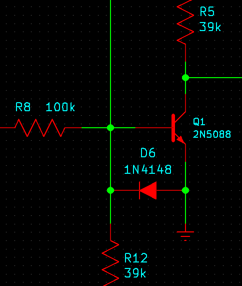
Note the diode D6. That is there to protect the base-emitter junction of Q1 from any reverse voltage that might be applied. In normal operation, the base will be driven (through R8) from a Eurorack gate pulse, which is typically between 0V and +5V, so Q1 would never see a negative voltage on its base, reverse-biasing the base-emitter junction (bearing in mind that the emitter is fixed at 0V). Even if someone plugged in something like an oscillator output, which might typically go to -5V, the voltage divider between R8 and R12 would limit the negative voltage on the Q1 base to -1.4V, which is not enough to be a problem for Q1. A lot of people designing cut-price Eurorack modules would call that good enough and save the few cents' cost of the diode and the (probably more expensive) board space it consumes.
But one of the principles I follow in my designs is to do it right, and that means considering that someone might plug a -12V power supply into the input of my envelope module. What happens then? Such a voltage through the R8/R12 voltage divider works out to -3.37V applied to the transistor base, which is only rated for -3.0V. Since the data sheet rating is somewhat conservative, it might still be okay; and even if the transistor did go into breakdown mode, the 100kΩ resistor would keep the breakdown current pretty small. Probably, the module would survive even without D6. But damage from that kind of thing can build up over time, and I don't want customers blaming me if they heavily abuse the module and it breaks, so I designed in a protective diode. Long before the voltage on the base of Q1 goes far enough negative to be a problem, D6 will become forward biased and keep the voltage limited to about -0.6V. The module (although only officially rated down to -12V) should tolerate several hundred volts of negative input; beyond that, the most likely place for it to fail would be due to arcing in the input jack socket.
Something similar exists in the output buffer of the Transistor ADSR.
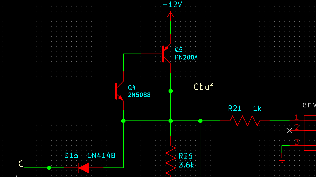
Here, the main issue is with someone connecting the output to a strong positive voltage. What happens if the output is shorted into the +12V supply? The connection labelled C can be driven to 0V pretty hard during some phases of the envelope cycle, so in the worst case that would be putting about 8.8V (taking into account the other loads at the emitter of Q4, which form a voltage divider with R21) of reverse bias across Q4's base-emitter junction, which again is rated for only 3.0V. To make matters worse, there isn't much current-limiting here, because R21 can't be made much bigger without harming the output impedance, and I can't really switch to a different transistor type that would handle more reverse voltage because at this point I really need the high gain of the 2N5088 to avoid placing much load on the envelope capacitor. This is another case where it makes sense to add the protection diode, D15 - and check carefully the other parts of the circuit to make sure that the current through it will not damage those either. This is another of the little details that make North Coast Synthesis modules superior to some of the others on the market, because a lot of module designers, even those with flashy fibreglass panels and with an appearance of professionalism, would leave it out and call the output driver "safe enough when not abused."
So if protective diodes between the base and emitter are so cool, why aren't they just built into all transistors, making it unnecessary for designers to pay attention? With some high-power or high-performance transistors, they are. The MAT12 transistor pair from Analog Devices, for instance, is two precisely matched transistors in a can with built-in protective diodes, to guard against damage to their base-emitter junctions from accidentally applied reverse voltage. Having the diodes built in makes it impossible to run the transistors upside-down in reverse active mode, but it's rare that anyone would ever want to do that anyway. A more important reason not to do it is that the protective diodes, mildly reverse-biased during normal use, add a tiny leakage current and a possibly significant amount of stray capacitance to the base of the transistor. At high frequencies (far higher than audio) that stray capacitance can cause a number of problems for frequency response; even at audio it may occasionally contribute to stability problems. So although often a good idea, protective diodes cannot just be thrown in everywhere. Like most things in engineering, there is a trade-off involved.
Why is NPN more common?
When people talk about bipolar transistors, they usually talk about NPN transistors as the default, with little or no mention of the other kind. I'm guilty of that myself in this article, mentioning PNP transistors only in this little section at the end. Why the bias, pardon the pun?
It's an observed fact that NPN transistors are more common in general use. The North Coast Transistor ADSR uses both kinds, but the Transistor Mixer uses only NPN transistors, and the same is true of very many other transistor circuits you can find on the Web - at least as long as we're talking about silicon transistors, which is a clue to part of the story.
We might say that NPN transistors, which like to live near the negative supply voltage and have bias networks built up "above" them, are better suited to the typical situation of a single positive supply and 0V; but that argument is circular, because it might just as well be said that that power supply arrangement is so typical because it's what works well with NPN transistors and if we had a reason to use mostly PNP transistors, we'd use power supplies arranged the other way around. Indeed, old guitar-pedal designs which do use PNP transistors, often use exactly the kind of "backwards" (compared to modern practice) power supply you'd expect, with a 0V rail and a -9V rail. So power supply seems to be more an effect, not a cause, of the preference for NPN.
The first thing to understand is that although we talk about "doping" as an abstract process and draw nice little round-corner diagrams and label the regions N and P just as if they're equal and opposite to each other, the actual experience of making doped semiconductors is incredibly messy, poisonous, and difficult. First you have to make the basic semiconductive substance itself - silicon, germanium, gallium arsenide, or something more exotic. This stuff has to be incredibly pure before you start doping it; even after being "heavily" doped it is still one of the purest substances human beings manufacture on an industrial scale, and the starting point before adding the dopants is much purer than that. Quite often, the purest silicon you can manufacture will still be mildly P-doped by natural impurities such as aluminum, and you have to compensate for that in your deliberate doping.
To dope silicon into N-type, you might add phosphorous or arsenic; for P-type, you'd usually add boron. (Other dopants are possible for silicon, and others yet might be used for other semiconductors than silicon.) Each dopant has its own unique chemical properties and may require different techniques to get it into the silicon. Also, depending on your manufacturing process, you may be adding one dopant even to parts of the die that you actually want doped the other way, then adding another in limited spots to compensate. The bottom line is that it may not be equally easy to do N-type and P-type doping; and so it may be harder to build good PNP silicon transistors than good NPN ones. That would make PNP transistors more expensive for the same performance, and quickly drive the industry to standardize on NPN.
That kind of thing is probably the reason PNP germanium transistors were more popular than NPN germanium transistors Back In The Day. Even now if you go shopping for germanium transistors, the decent ones will almost all be PNP. I think the chemistry for doing N- and P-type doping of germanium favours manufacturing PNP type, and there's no reason something similar might not favour NPN in the case of silicon. However, I don't think that's the main reason NPN silicon transistors are the more popular kind today. Now is the twilight of the bipolar transistor age; we are still working on lithography for building smaller and smaller MOS transistors, but I think we're about as good at plain old silicon doping for bipolar transistors as we will ever be and given the usefulness of having both kinds it's surprising for differing manufacturing difficulty to still create a strong emphasis on NPN.
The bigger reason for NPN to be favoured has to do with speed. Discussions of basic transistor operation usually treat electrons and holes as exactly equal and opposite, but they really aren't. An electron (or maybe the electron) is a physical object that actually moves with the flow of current by careening through the crystal, though the abstraction of current, as wave-like pressure of electrons, moves faster than the physical electrons themselves. A "hole" in semiconductor physics, as the space where a valence electron "ought" to be according to the crystal structure of the material, is not a physical object and moves in a more complicated way. First a nearby electron has to move into the hole, creating a space behind it; then another one has to move into that; and so on. The result is that movement of holes is slower. And although both kinds of charge carriers are needed by both kinds of transistors, NPN transistors use electrons where PNP transistors would use holes, in such a way that (at the limits where this effect overcomes other issues) NPN transistors are capable of operating faster. That creates a reason to prefer NPN transistors in high-frequency applications, and then other advantages of everyone preferring the same kind of transistor cause the preference to extend even into applications like audio where speed is not really a big issue.
◀ PREV Tools for getting started with SDIY || Transistor ADSR release NEXT ▶