AC and DC coupling
2023-03-28 electronics design
I overheard somebody asking about the plusses and minuses of DC coupling, and AC coupling capacitors, and being told to read the detailed explanation of such things I'd written on this Web site. I was flattered to think the speaker found my article helpful, especially because I'd never actually written one about that!
Thinking that there was evidently demand for such an article, I started working on one and it quickly grew to be longer than would make sense for a single posting, so I've split it into three. (EDIT: probably four.) This is Part 1, introducing the issues and going into some detail on AC coupling. In future installments I'll talk about electrolytic capacitors in particular, and some of the details of DC coupling.
Looking for solid ground
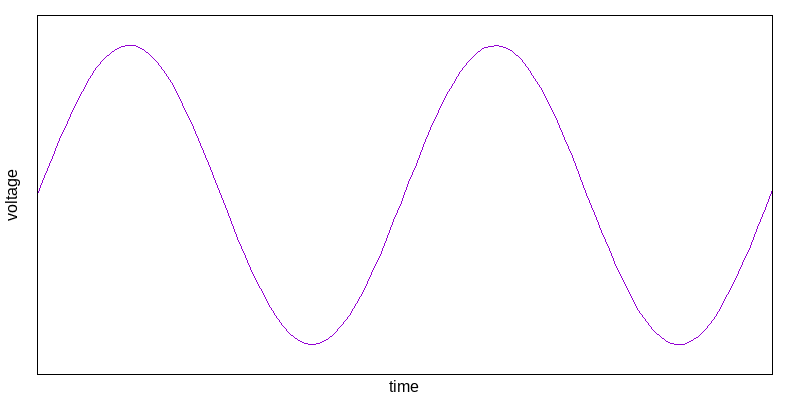
In analog electronics we usually think of a signal as something like what's shown in this picture. The voltage wiggles up and down and the interesting thing about it is the pattern of those wiggles.
I have not marked the actual voltages on that diagram. There is the word "voltage" off to the side suggesting that the voltage probably gets more positive toward the top and more negative toward the bottom, but exactly by how much, and what the specific voltages are at the top and bottom, is not specified. As I've written before, "voltage range" is usually the wrong way to think about signals and the vague picture above is often good enough for rock'n'roll, or more specifically, for playing music on a modular synthesizer.
The signal can be understood as a combination of two voltages: there is a constant voltage in the middle that we can think of as where the signal rests, and there is some amount of movement on either side. The resting voltage, which might well be zero when measured against some reference, is called the DC component, and the moving part is called the AC component. The abbreviations are for "direct current" and "alternating current," even when used, as here, to describe voltages rather than currents.
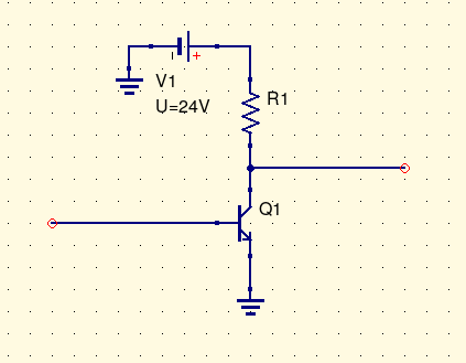
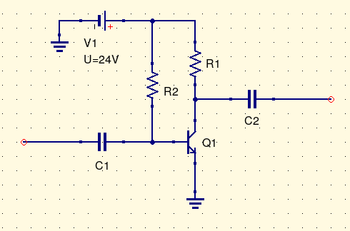
When designing a circuit that will process this signal, then we need to think about the specific values of the voltages. For example, consider this circuit, which is about the simplest transistor amplifier possible.
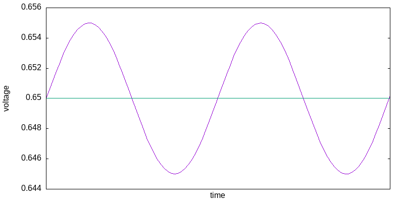
The basic rules of transistors say that in ordinary operation the base of this NPN transistor, connected to the input of the circuit, will sit one "diode drop" above the emitter, which is at 0V. A typical diode drop might be 0.650V. That is the DC component; the resting voltage of the transistor base when the input is silent. Applying a signal will temporarily raise and lower the base voltage, wiggling it around this centre. When actually designing the amplifier it might be more convenient to describe the signal at the base in terms of current, but the effect of a strong input signal on the voltage might be to move the base up and down by ±5mV, so covering a range from 0.645V to 0.655V, as shown.
As the base voltage varies a little, the current through the transistor Q1 from collector to emitter varies a lot. That current passes through the resistor R1, which drops a varying amount of voltage depending on the current. The voltage at the output is 24V (the power supply) minus whatever amount is dropped by R1, and it might look something like this.
Note the different voltage scale markings. What was a 10mV range of variation on the input has become a 4.7V range in the output: the amplitude of the signal (as measured strictly by voltage) has increased by almost a factor of 500. The circuit has significantly amplified the signal.
Sharp-eyed readers may note that as well as being inverted, my diagram of the output voltage is slightly asymmetrical. That is because it's meant to represent the actual performance of the amplifier, which would be overdriven a little by the signal level in my example. Raising the transistor's base a few millivolts makes it conduct more current, which makes the resistor drop more voltage by Ohm's Law. Slightly higher input voltages mean significantly lower output voltages; the gain is negative. But because of the exponential response of the transistor, the negative gain has greater magnitude when the base is at a higher voltage, and less when the base is at a lower voltage, so the peaks of the output waveform get a little pointier in the negative direction (at higher input voltage). This effect would be audible as even-harmonic distortion if you were listening to the output.
But as well as amplifying and slightly distorting the AC component, the circuit has also changed the DC component. Whereas the input was centred on 0.650V, the output is centred on about 11.85V.
If you want to be the next Randy Bachman and plug the output of an amplifier into the input of another amplifier, then the amplifiers involved cannot be designed exactly as shown here. You won't get good results putting a signal with a DC component of 11.85V into the input of an amplifier that's expecting a DC component of 0.650V. Depending on the power and resistance specs of the resistor R1, either or both amplifiers might end up fried, and at the very least, neither of them will be operating normally.
Designing a system with multiple stages of circuitry that each have their own DC levels for input and output quickly becomes complicated. We constantly have to know the DC level at each point, and think of ways to shift it if it's not what the next stage requires. Note that although possibly related, this is a separate issue from the level of AC signals or the impedance of the connection. Amplifiers in real life are not so simple as the single transistor and resistor shown above. They contain additional components that, among other functions, move the signals to appropriate DC levels for interfacing with other stages.
It gets even worse when the DC levels of signals are inconsistent and unknown. I described the DC component of the Q1 base voltage as 0.650V in my example, as a "typical" diode drop. But really, it depends a lot on the temperature. The optimal voltage gets lower as the transistor warms up. If we tried to hold the input voltage absolutely fixed, then if the transistor got hot the base voltage it was looking for would decrease, making the input too high, and in some circuits then the transistor would start passing more current, which would heat it up to an even higher temperature, in a compounding effect called "thermal runaway" that might end with the transistor exploding.
In my example circuit the resistor R1 will probably never allow the transistor enough current to destroy itself, but even when thermal runaway is excluded by the circuit design, there are problems in the variation from one individual transistor to another. The input voltage that is perfect for one 2N3904 might not be quite right when we build another copy of the same circuit with another 2N3904. There is variation on the output as well: I said the output DC level was 11.85V but it depends on the gain of the transistor and on how we resolved the issues at the input, so it's quite likely that the real DC level of the output will be only approximately 11.85V. Not knowing the precise DC level that the circuit expects at the input or produces at the output makes it all the harder to interface it with other circuits.
At this point we are facing one of the fundamental problems of electronic design. How do we get a signal at one DC level from the output of one stage to be on a different DC level for the input of the next stage, when these two levels may be quite different, and we don't actually know what they are, and they can change?
Using zero
One solution that might seem reasonable would be to standardize the DC level for signals. If we just pick a level and insist that every circuit should expect and produce that level, then we have one less thing to worry about when connecting them. And the consistent level that seems to make sense to use as the standard seems like it should be zero. Every circuit that uses basically AC signals, should make them pure AC with the DC component equal to zero. Problem solved, right?
In practice, although we quite often do want to use zero as the standard DC level, really achieving that is not so simple and it may not be the right call everywhere. The first problem is that it's hard for any circuit to handle voltages outside its own power supply range. If we're using, as in the example circuit of the previous section, a power supply with voltages labelled "0V" and "24V," then in order to produce a 4.7V peak-to-peak signal centred on 0V, the circuit is going to have to momemtarily produce a voltage of -2.35V on the output. Where will that negative voltage come from?
To a first approximation, it's impossible for a circuit's output to be outside the range of its power supplies. You can amuse yourself by trying to list all the exceptions to that statement. There are many, but none of them trivial. Traditional transistor circuits have trouble generating output voltages that are even close to the power supplies, let alone outside. So the amplifier will have a hard time producing the momentary negative voltages needed if we have zero as the reference level.
After one stage manages to produce a negative voltage on its output, it's also going to be a problem for the next stage to take that negative voltage as input, for similar reasons. Apply a negative voltage (that is, a voltage below the emitter) to the base of a transistor as in my example circuit, and the base-emitter junction will be reverse-biased, taking the transistor out of normal amplification mode. Input centred on zero will definitely not be what the transistor wants, and we will have to shift it somehow to make the amplifier work - as we would probably need to do anyway, but the point is that nothing has been saved here by choosing zero as the standardized DC level.
The problems with using zero as the standard DC level actually come about not because zero is a bad DC level in itself, but because zero happens to be one of the power supply voltages and it's bad to use a power supply voltage as the reference. So what if we moved the power supplies away from zero? It is not necessary to call the two power lines driving the amplifier "0V" and "24V." We could just as easily change the labels on those wires to read "-12V" and "+12V." The circuit would still operate the same way. Then 0V would be right in the middle, at a voltage the circuit can much more easily handle. Note that the "11.85V" output DC level in my original example is already very close to the midpoint of the positive and negative voltages, which is now called 0V.
And that is, in fact, what's usually done with analog Eurorack circuits. We have a power supply that is in some sense 24V, but the two main power lines are not called "0V" and "24V"; rather they are "-12V" and "+12V." It is expected that the DC reference for signals will be midway between them: 0V. Module designers are expected to arrange their circuitry so that inputs will correctly handle signals centred on 0V and outputs will produce signals centred on 0V. It's relatively easy to design transistor circuits to handle signals centred near the midpoint of the power supply lines, and so the requirement on module-to-module communication is to do exactly that.
It's still necessary to deal with things like the changing value of a transistor's "diode drop," but there are common design techniques that work well for that. A lot comes down to using differential signalling. Instead of the circuit having its own preferred DC level for the signal input, we will build the circuit to have a extra input line through which we tell it what DC level to use. Then we distribute a reference level, often thought of as a third power supply rail at 0V, throughout the system, and we expect everybody to use that.
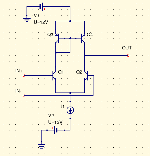
Instead of having just one transistor and one input in the front end of an amplifier, we might use a pair of them, as shown here.
The transistors Q1 and Q2 are in the classic "long-tailed pair" configuration. If the two inputs labelled "IN+" and "IN-" are at the same voltage, then the two transistors (assumed to be identical) will float their shared emitter to some voltage that is unknown and variable, but about 0.650V below the input. The current from the current source I1 will be equally split between the collectors of Q1 and Q2. This is true as long as IN+ and IN- are at the same voltage, within a reasonable range, no matter what that exact voltage is, and it remains true as the characteristics of Q1 and Q2 remain matched even if changes in temperature change their diode-drop voltage. Raise or lower the base of one relative to the other and the division of current between them will change, according to the difference in voltage between the two bases rather than the absolute voltage. Normally one of these transistors would be connected to 0V and the other would receive the actual signal.
The additional transistors Q3 and Q4 form a current mirror, which recovers useful information from the variable split of current between Q1 and Q2. The overall circuit has current-mode output: it will either push or pull current through the output wire in an amount and direction that is controlled by the voltage difference between the two inputs. And the current at the output is another thing that does not depend much on voltage: it can drive whatever is downstream at any of a wide range of voltages without much change in its own operation. So this circuit is a building block for designing things that will be relatively immune to DC level issues.
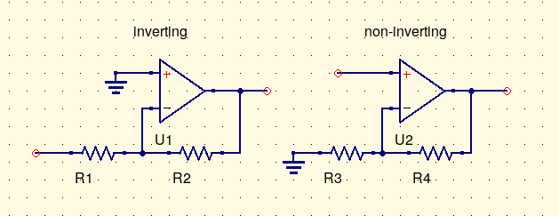
If you look at the internal circuit of almost any common op amp chip you'll see the inputs handled by a section much like the one shown above. In a typical inverting op amp configuration, the 0V line is connected directly to the op amp positive input. In a typical non-inverting configuration the connection to 0V is indirect, but it remains that 0V is being used as the reference around which the input signal gets multiplied. Either way, the point is to use a DC level in the middle of the power supply range, and give that level to the circuit as an input that can be shared across the whole system, keeping it consistent throughout, instead of having each section invent its own reference level.
The op amp is not a complete solution to DC level issues. We can't always use an op amp; and anywhere we aren't using an op amp, there are still DC level issues to deal with. The people who design the op amp chips still face DC level issues inside the chips. If the transistors in a differential pair are not perfectly matched - and manufacturing tolerances mean they are never perfectly matched - then the op amps themselves may introduce DC offsets, because they are effectively working from a reference level that is not quite 0V. These offsets can be compounded as signals get amplified through additional stages. Requiring a split power supply for the whole system and distributing a separate 0V line everywhere increases the complexity of the system, especially when (as happens in Eurorack in particular) designers start using that 0V line as a power line too, not only as a reference level. By going to a split power supply with 0V as the reference, we may be only replacing some problems with others.
Adding a capacitor: AC coupling
What if there were a component that would add or subtract a voltage corresponding to the difference in DC level between input and output, allowing the AC part of the signal to pass through unchanged? What if it would also automatically detect the right amount of DC to add or subtract, and adjust when the desired levels changed? Then we could put one of those between an input and output that had different DC levels, and our problems would all be solved.
In fact, an ordinary capacitor can do all that - subject to some important limitations.
Suppose we connect a constant voltage of 11.85V to the input of this circuit, the left side of C1. The right side of C1 is held at the transistor's base voltage, about 0.650V. Current will flow as the capacitor charges up to the difference between the voltages (11.20V). That takes a certain amount of time; but after the capacitor is fully charged, it holds its voltage without further current flow.
If the input voltage changes rapidly, the capacitor doesn't have time to charge or discharge. Lower the input voltage 5mV very fast, and the transistor base voltage goes down 5mV too, because the capacitor is holding a fixed difference between its two ends. The same in the other direction.
But if there is a slow change in the voltage, the capacitor will have time to charge or discharge (with a small current flowing through it during that time). If over the course of a few minutes, the DC component of the input signal slowly changes from 11.85V to say 12.30V, the voltage across the capacitor will just increase to the new difference.
Rapidly-changing signals, that is, AC, make it through the capacitor with little or no impediment. Constant signals, that is, DC, are blocked. Slow changes in the DC level have no significant effect; the capacitor automatically adjusts to them. The input and the transistor base are each allowed to seek their own DC levels, and the capacitor neatly shifts the AC part of the signal from one DC level to the other.
Because the capacitor C1 blocks any applied DC on the input from making it through to the base of the transistor, we cannot depend on the input voltage to set the bias; that is, the base voltage I've been calling 0.650V which determines the normal level of current through the transistor when there is no applied signal. If the capacitor were the only thing connected to the base, allowing no DC current flow, then the transistor would basically be shut off by default. Its base voltage would be too low. I have drawn in the resistor R2 to represent a very simple bias arrangement. A small current from the power supply will flow through this resistor into the base of the transistor, raising the base voltage a little and allowing a larger current through the collector to set the operating point. This single-resistor bias will be sensitive to variations among individual transistors and, with a single transistor, temperature changes. A real amplifier would probably use a more elaborate bias circuit, but that would only complicate the discussion of coupling.
Using a capacitor between stages is what people usually mean when they say AC coupling. The capacitor itself may be called a DC blocking capacitor. The alternative, when you're not using a capacitor but just directly connecting the stages so they will pass changes in the DC level from one to the next, is usually called DC coupling. The core of the distinction is that with a capacitor, only the AC part of the signal passes through, whereas without a capacitor, the DC passes as well.
The terms "AC coupling" and "DC coupling" are a little bit nebulous. Some people want the "DC" in "DC coupling" to stand for "direct coupling," apparently because they think "direct coupling coupling" makes more sense than having DC coupling be the coupling that allows direct current (DC) to pass. There are also other ways to exclude DC than using a capacitor. For instance, you could use a transformer, which will similarly pass AC and not DC. Using a transformer seems like it might literally qualify as AC coupling, but it doesn't involve a capacitor, and people almost always expect the term "AC coupling" to refer to a capacitor in particular. It might be best to say "transformer coupling" when that's what you mean, to prevent confusion. A further possibility would be to use optical coupling, with a light source and light detector to get a signal from one circuit to another without any flow of electricity between them, as in the famous Vactrol.
AC coupling is flexible, and basically automatic. Add the capacitor and you're done. It's not necessary to know exactly how much DC voltage difference you're blocking, and that's important because you may not be able to know. The voltage difference can change depending on individual components, with temperature, as the user patches into different modules, and so on. Trying to guess the voltage difference once and for all is brittle. Your guess could be wrong, or could become wrong when things change. Building a circuit to automatically adjust to changes in DC level, other than just putting in a capacitor, might be difficult and expensive.
AC coupling means we can use a DC reference level of 0V even in single-supply circuits where 0V happens to coincide with one of the power supply rails. That is standard practice with guitar pedals, for instance. The pedal circuit will normally be built to use supply voltages of 0V and 9V. If it needs to use op amps or similar circuitry, it may generate a reference level for them somewhere in between (such as at 4.5V), carefully using that only as a reference and not a supply line. The input and output are expected to use reference levels of 0V, but the pedal circuit doesn't even need to care exactly what DC references other circuits are using, because it will have AC coupling capacitors at both input and output, automatically adding or subtracting the 4.5V or other appropriate voltage to translate the levels.
AC or DC?
The biggest disadvantage of AC coupling is that the capacitor really will block DC, as it's meant to. If the signal you want to transmit makes important use of specific DC voltages, the coupling capacitor will not pass those voltages through. In modular in particular, this issue comes up in the context of control voltages. Except for a brief charging transient, there is no difference between connecting a constant 0V or a constant 5V to an input with a coupling capacitor; the downstream module won't see the difference between 0V and 5V. So it's a disaster if you try to patch something like a slowly-changing pitch or volume CV through a module that uses AC coupling; all the information will be lost when the signal comes out the other end.
Because of the desire to pass through control voltages unchanged, AC coupling has something of a bad name in some modular circles. Synth users often want their modules to be "DC coupled" as a matter of course and they see that as a selling point. "List of DC coupled audio interfaces in [year]" is a perennial forum topic, and I think at least some people posting in such threads believe the only difference between a DC-coupled and an AC-coupled circuit is the presence or absence of a gratuitous capacitor that really ought to just be left out to make the circuit better. More on DC-coupled audio interfaces in Part 3 of this series. I hope by this point I've made it clear that AC coupling capacitors do address a real problem and they are not only built into equipment to annoy wigglers.
If you're designing with op amps and you have positive/negative split supplies, then simple functions like amplification and mixing are reasonably easy to do in a DC-coupled way with zero voltage as the reference, and that is the usual practice in Eurorack. There are still some issues with DC level in these circuits, because of the offsets introduced by the op amps. It may be that the level gets shifted a few millivolts each time the signal passes through an op amp, which could be three or four times for each module on average, so that a signal perfectly centred on zero could be off centre by a fraction of a volt after a few stages of mixing and processing.
Accumulated offsets can be a problem in very precise DC control voltages, such as those used for pitch control. An amplitude control voltage fed into a linear VCA might fail to "close" the VCA when silence is desired, if offsets have shifted its zero point above the 0V reference. Most modular designers and users seem to prefer DC coupling with op amp circuits nonetheless. The ability to run fixed control voltages through the same modules as audio seems highly valued.
If you're designing with discrete transistors, on single-sided power, or if you're interfacing with digital systems that also use single-sided power, it may be another story. Transistor circuits like the ones in my examples above really need to have their AC signals riding on the right DC voltages, those voltages will usually be different between input and output, neither of them being a convenient "zero" offset, and the offsets will change a lot with temperature and for other reasons. It is hard to build a basic transistor amplifier that works well at DC. I made some attempt at that in the Transistor Mixer, but it still needs trimming for offset, and I ended up including both a DC- and an AC-coupled output to give users a choice. I myself usually use the AC-coupled output on mine. AC coupling makes a lot of sense for basic transistor circuits. Similarly, ADCs and DACs can usually only handle voltages between the microprocessor power rails (typically 0V and 3.3V), and they try to keep analog signals centred at the halfway point of that range; not at zero.
I decided to make both the Leapfrog VCF and the Coiler VCF DC coupled, so they can be used with arbitrarily slow control voltages. That seems to have worked better with the Leapfrog than with the Coiler. I wanted the Coiler in particular to be DC-coupled so it could operate as an envelope follower, but when people have trouble with their Coilers it often turns out to be because of DC offset issues, which would probably be at least reduced in a circuit with a few more DC-blocking capacitors.
Frequencies and capacitor values
An AC coupling capacitor is supposed to let through AC and block DC; but what, exactly, are AC and DC? Theoretically, a DC signal is one of zero frequency: a voltage that never changes in all of eternity. Such a voltage does not really exist. At some point in the future you'll have to connect or disconnect the input, flip the power switch, get on a rocket ship to escape the surface of the dying Sun as it encompasses the Earth's orbit, or similar. All we ever really have are voltages that change. Some change faster than others. We call the fast ones AC and we call the slow ones DC.
The AC coupling capacitor can be thought of as the "C" in an RC high-pass filter. The "R" comes from the prevailing impedance of the connection where we installed the capacitor. This filter will have a cut-off frequency. Signals that change at rates well below the cutoff, we will consider "DC," and they will be blocked by the capacitor. Signals that change at rates well above the cutoff, we will consider "AC," and they will pass through. Signals near the cutoff will partially pass through, but will be attenuated, and attenuated more as the frequencies get lower until we're into the range where we can think of them as being blocked completely.
The important question in designing a coupling capacitor, then, is what the cutoff frequency ought to be. That will determine the capacitor to use.
The cutoff frequency ought to be significantly less than the lowest frequency we want to pass through the coupling, while still significantly higher than anything we want to block. Usually it's the upper limit that is more significant. You rarely end up with any danger of the cutoff turning out too low. Audio goes down to about 30Hz, so a reasonable target for cutoff frequency in an audio circuit might be 10Hz or less.
The formula for cutoff frequency of an RC circuit is f=1/2πRC, where f is the frequency in Hz, π is 3.141592..., R is the resistance in ohms, and C is the capacitance in farads. Normally for "resistance" you want to use the sum of the impedance of the input and output on either side of the coupling capacitor. Often the input impedance will be much larger than the output impedance, so the sum is basically just equal to the input impedance.
To calculate the capacitance target, we can rearrange the equation to get C=1/2πRf.
For example, if it's desired to couple a Eurorack input and output with 1kΩ output impedance, 100kΩ input impedance, and a cutoff frequency of at most 10Hz, then the formula works out to C=1/2×3.141592×101kΩ×10Hz, which is 0.157µF. It would be reasonable to round it off to 0.15µF, which is a common preferred value.
There are some pitfalls in this kind of calculation. First, this is a one-pole high-pass response, with neither a sharp knee nor a steep slope. It doesn't block everything below and pass everything above the cutoff, but shades slowly from one to the other. Frequencies at or near the cutoff frequency will be somewhat attenuated (-3dB at exactly the cutoff, by definition), and so you need to set the cutoff significantly below anything you want to pass through unchanged. On the other side, even frequencies a fair bit below the cutoff will still pass through a little, so if there are any slow changes that you really want to be sure of blocking, then the cutoff needs to be set significantly above them.
If you happen to patch together an input and an output that both include coupling capacitors, then the two capacitors are put in series, resulting in an equivalent capacitance smaller than either of them - and therefore a higher cutoff frequency. Not knowing what other designers are doing, a reasonable guess might be that they will be making capacitor decisions similar to your own; and then you end up having to double the calculated capacitance value for your target cutoff frequency, to make up for the way it will be halved by the series connection.
For a high impedance like 100kΩ the target capacitor value is manageable, but the capacitance C for a given frequency f increases as the resistance R decreases. In lower-impedance circuits, the necessary capacitor may be quite large both in capacitance value and physical size. The worst case might be something like the output of a power amplifier that drives a subwoofer: very low impedance like 4Ω, and cutoff frequency at the very bottom of the audio range. The calculated capacitance ends up being thousands of µF, and at that point it may not be the right choice to use capacitor-based AC coupling at all. Real output stages for subwoofers are likely to use other techniques, such as transformer coupling, instead.
When things are not quite so extreme and you still want to use a coupling capacitor, it may be necessary to use an expensive capacitor, to use a capacitor that is not the type you're otherwise prefer (such as electrolytic or high-k ceramic), or to compromise on the cutoff frequency and let it be a little higher than you'd otherwise choose. In the Transistor Mixer I opted for an expensive and physically large 4.7µF film capacitor, partly covering its cost in the fact that the minimalist design saves some money on the other components by having few of them.
Electrolytic capacitors are often appealing for AC coupling purposes when a large value is needed, and they raise some unique issues of their own. I'll describe those issues in Part 2 of this series before giving some thoughts on DC coupling in Part 3.
◀ PREV New Gracious Host firmware ideas || Electrolytics for AC coupling NEXT ▶
