More about DC coupling
2023-04-02 electronics design
In earlier articles I've talked about the general issues of AC and DC coupling, and some specific considerations for using electrolytic capacitors. This third article of the series will look at DC coupling in particular.Operational amplifiers ("op amps") are popular analog building blocks, especially in synthesizer electronics, because it's easy to analyse what they do to voltages. The first rule of op amp analysis is that (in negative feedback configurations, and when this is possible) the amplifier moves its output voltage in order to make its input voltages equal. That is useful in building circuits to manipulate DC voltages.
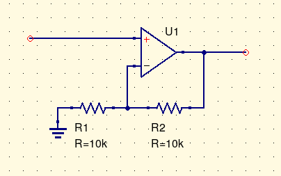
For instance, in this example the resistors form a voltage divider that cuts the output voltage in half. The op amp adjusts its output so that half the output will be equal to the input - which means the output is exactly twice the input. That works at all frequencies the op amp can handle, including down to DC (0Hz), and the gain is set by the resistor ratio without any need to go into details of the op amp's specifications. This kind of circuit lends itself to DC coupling. Trying to build a voltage-doubling circuit that worked at DC with discrete transistors would be much more complicated.
The bias current capacitor-charging trap
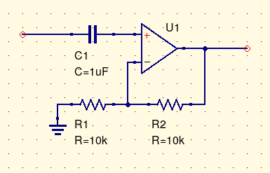
Although op amps tend to work well with DC coupling, sometimes people want to build AC-coupled op amp circuits anyway. Maybe you're concerned about DC offsets introduced by other modules and want to re-centre the signal on zero; so you add a capacitor at the input of the above non-inverting voltage doubler to block the DC and hope that the circuit will double just the AC voltage.
That's not going to work! Exactly what happens depends on the op amp chip and the size of the capacitor, but the typical syndrome with this kind of circuit is that when you first turn it on, it appears to work, but then over the course of a few seconds it first starts to exhibit a lot of distortion, and then the signal cuts out entirely. Turning it off, leaving it off for a while, and then turning it on again, usually "resets" it to work for a few more seconds before cutting out again. What is going on here?
The problem is with bias current. One of the rules of op amp analysis is that the current through the op amp inputs is zero; but that is only an approximate rule. Really, there is always some small amount of current, called the bias current, which flows through the inputs. In the case of a JFET-input op amp like a TL074, the bias current is flowing through a reverse-biased PN junction, which basically functions as an insulator, and so the current is very small. For a traditional (not "-H") TL074C it's up to 7nA over the full temperature range, up to 200pA at 25°C. An old-fashioned op amp built with bipolar transistors, like an original 741, might have up to 1.5µA of bias current over the full temperature range. Some CMOS op amps designed specifically for low bias current, like the Analog Devices ADA4530-1, may have as little as 20fA of bias current. That's 20 "femtoamps," or 0.00000002µA.
Regardless of the amount, what the bias current does in this circuit is it charges up the capacitor. There is nothing else to set the DC level on the op amp's side of the capacitor; so over time, usually a few seconds, the DC level will move toward one power line or the other (which one, depends on the direction of the current), and eventually it's at such a high or low voltage that the op amp can no longer handle it and stops working. Another way to look at it is that the capacitor allows different DC levels on its two ends, and in this circuit there's nothing that actually sets the DC level on the side of the op amp input, so it can float to an unhelpful voltage.
Bias currents and resistors
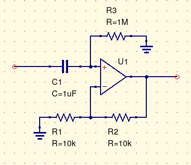
A simple rule to avoid the capacitor-charging problem is that there must be a DC path for the bias current from every op amp input to something that can handle the bias current. Using an inverting instead of a non-inverting configuration would work, because then one input would be grounded and the other would be connected to the feedback resistor and through that the op amp's own output; we can basically add an AC coupling cap to an inverting amplifier with impunity. If it's important to keep the non-inverting configuration and AC coupling, we might add a high-valued resistor to ground (or to whatever voltage is chosen as the reference level), just to make sure the DC reference remains under control.
The resistor value needs to be appropriate for the amount of bias current involved. With a 1MΩ resistor and the TL074's maximum bias current of 7nA, the voltage drop across the resistor and therefore the DC reference at the op amp's positive input ends up being up to 7mV away from zero. If that is too much, then a lower resistance value might be needed. But this resistance (which is much smaller than the effectively infinite impedance of the op amp input) ends up setting the circuit's input impedance, so there's a tradeoff in reducing it.
The trend to small bias currents in modern op amps means this next bit isn't usually done anymore, but in some designs that use older or special op amps with relatively high bias currents, people will attempt to equalize the DC impedance seen at the two inputs of the op amp - for instance, with a resistor to ground for an op amp input that would otherwise be directly grounded. That way, assuming the bias current is equal on the two inputs, the voltage offsets created by the bias current will also be equal and will cancel out. The op amp may have some other sources of offset, as described below, but if the offset resulting from bias current was the biggest factor, then equalizing the impedance might be useful in minimizing its effect.
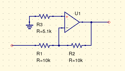
In this inverting amplifier the voltage divider of two 10kΩ resistors creates an impedance of 5kΩ (by parallel resistor calculation) visible at the op amp negative input. I've drawn in a 5.1kΩ resistor for the other input as the nearest convenient standard value to 5kΩ, and close enough. The equality of the bias currents between the two inputs is only ever approximate anyway, so there's no point investing too much effort in making the resistor value exact. In some cases, especially if using higher resistor values, some designers might also add a bypassing capacitor in parallel across R3 to make sure that the op amp input is solidly grounded with respect to AC signals.
Op amp offsets and trimming
The rule that an op amp tries to make its input voltages equal is another one that's only approximately true. Usually each input drives the base or gate of some kind of transistor (BJT, JFET, or MOSFET) in a differential pair; and although there will be some effort made to make those transistors identical between the two inputs, there is inevitable manufacturing variation. The op amp's target is to make the two transistors pass equal current, and if the transistors are not quite identical, it may be that it will be perfectly balanced when the voltage difference between the inputs is actually some small voltage other than zero. That is called the offset of the op amp. This effect is separate from, and added to, any effect resulting from bias current and unbalanced impedances.
Incidentally, offset resulting from mismatch is one reason "discrete op amps" are usually a bad idea. Having the two input transistors on the same chip makes it much easier to match their parameters, and to keep them matched in the face of temperature variation. If you try to build an op amp with discrete transistors, on separate chips, it's much harder to keep the offset small - and the effect is compounded because other parts of an op amp, not only the input pair, also usually require matched transistors. The audiophile crowd have managed to convince themselves that "discrete" circuitry is a good thing, and I may be guilty of contributing to that perception with my own discrete-transistor mixer and ADSR products, but op amps are the wrong place for things to be "discrete."
Op amp input offset means that when a signal goes through a DC-coupled op amp circuit, it may come out with its average level shifted a little. If the op amp circuit was designed to double the voltage, it may be that the function it effectively computes is something like 2Vin+5mV instead of just 2Vin. If the signal passes through three or four op amps in each module, each one adding or subtracting a few millivolts, and the patch puts the signal through several modules, all DC coupled, then at the end of it the signal may be shifted by a big enough fraction of a volt for it to seem like a problem.
As references, the maximum specified offset of a traditional (not -H) TL074C over its temperature range is 13mV; for a 741 without use of the offset null pins it's 6mV; and for an AD8574 (a special low-offset device) it's 10µV. The fact that the long-obsolete 741 outperforms the more recent TL074C on this specification may seem surprising, but it's because the TL074C uses JFETs in its input stage, which are notoriously hard to parameter-match. As for how much offset is too much, we might note that one semitone on a V/oct Eurorack control voltage is 83mV. So it's reasonable, though maybe not a frequent occurrence, that a pitch control voltage routed through several levels of control, switching, and other utility modules could end up out by a semitone at the far end of the patch, just from uncorrected op amp offsets along the way.
Offsets can be a problem in DC-coupled audio filters in particular, where the signal passes around a feedback loop several times, hitting one or more op amps each time around, and there may also be relatively high-gain amplification that increases the effect of any offsets. Both the North Coast Synthesis MSK 007 Leapfrog and MSK 009 Coiler filters face this issue. More generally, it can be significant for any circuit that uses LM13700 or similar operational transconductance amplifiers into integration stages, because any offset in the LM13700 input leads to an unbalanced current output, which the integrator will add up into a steadily increasing voltage.
So it's a common practice, and done in both North Coast filters, to add trimmers (in the correct meaning of that term - not miniature panel pots) for compensating offsets. The idea is that after building the module, the builder can adjust the trimmer to add or subtract a little bit of voltage that will counteract the natural offset of the op amps, making the overall offset from the circuit input to output zero.
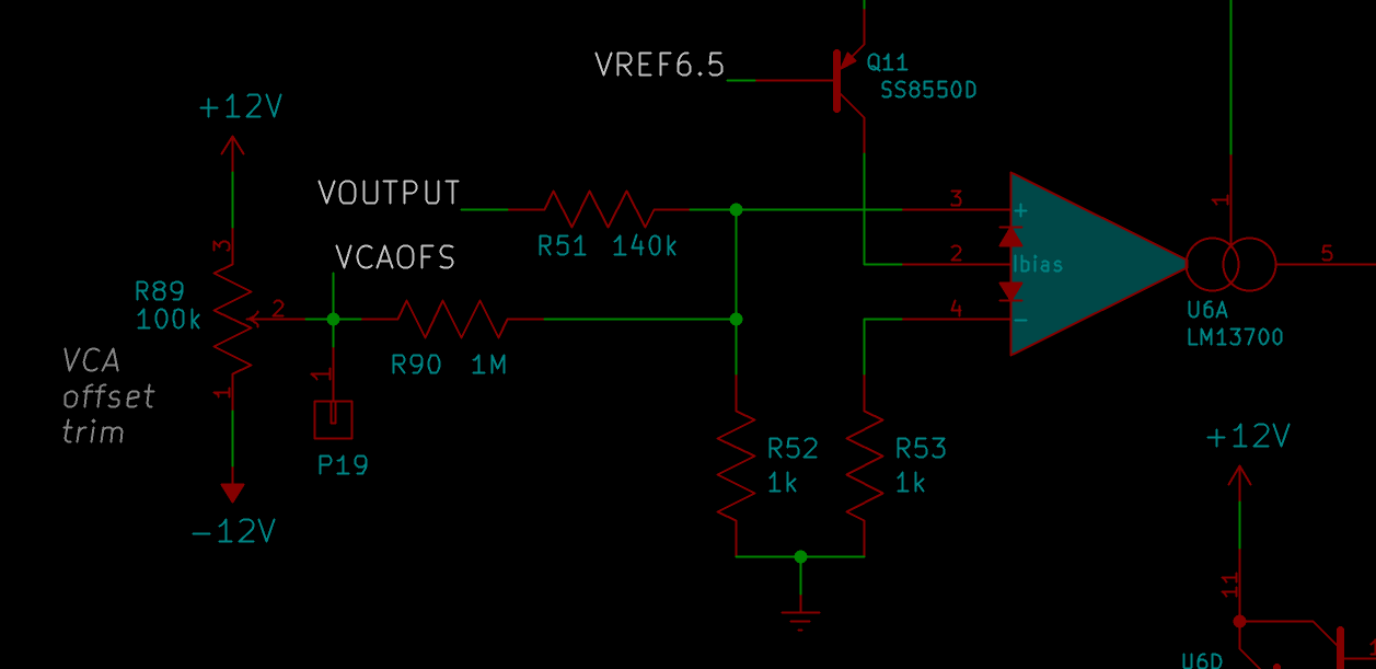
In the image, which is from the Leapfrog schematic, the trimmer R89 can be adjusted to a voltage of ±12V. That voltage is applied to a 1MΩ to 1kΩ voltage divider, so its net effect at the input of U6A is basically ±12mV. The LM13700's offset voltage is specified as at most ±4mV, but this trimmer is also meant to allow compensating for other offsets elsewhere in the circuit. Note that this circuit also uses the impedance-equalizing technique discussed above, in the shape of the 1kΩ resistor R53.
I used a similar technique in the MSK 008 VC Octave Switch, where the trimmers for the amounts to add and subtract in different octaves also indirectly control the offset through the module when used in straight-through mode. In that design I also used fancier op amps, TL074B type, where the -B suffix means they are selected for a little less maximum offset.
In principle every single op amp or other differential-input device (like an LM13700) in a circuit could have its own offset and could need its own offset trimmer. Actually building in that many trimmers is seldom practical or necessary. If a signal goes through several amplifiers in a row, it may be that the final offset is the sum of all the contributions of the individual amplifiers; and then just trimming one to bring the overall total to zero is good enough. When the gain relationships between the amplifiers are not fixed, that logic may not work perfectly. Offset in one place may not always have the same effect in another place where we might try to trim it out. But it still probably isn't really necessary to trim in every possible place; reducing the first-order effects may be enough to bring the overall total to an acceptable level of offset.
In the Leapfrog I decided to use just one trimmer for the "core" offset (applied to one integrator near the middle of the core) and I estimated that that would allow bringing the overall offset close enough to zero at all frequency settings, as to be good enough. Not trimming every integrator individually results in a little more control feedthrough, but it can still be adjusted to keep the overall offset close enough to zero. Really trimming them all separately would only make the already-complicated adjustment procedure even more cumbersome, and would add to the price of the module. The Leapfrog has a separate offset trimmer for the VCA section, which is the one shown in the schematic fragment above. The Coiler VCF, in which there's more issue of offsets adding up around feedback loops, has a separate trimmer for each of its two LM13700 sections.
Devil's advocate: do we really care about offsets?
One thing I've noticed about the Coiler VCF is that even though, from an engineering purist's point of view, it often has a pretty serious DC offset on its outputs, that's never what people complain about. The compromises necessary in that design to realize what might be called my artistic vision of a coil-based filter, mean that even with proper adjustment there may be a couple of volts offset in the output, as well as a fair bit of control feedthrough. That's just the nature of the beast.
When the trimmers get out of whack and there's a 5V offset on the output, and the customer emails me to ask for help, then the complaint I hear isn't "there's a 5V offset on the output." Instead, the customer says there is "hum" or "noise" in the output. The DC offset, which from an engineering point of view is the main issue, goes unnoticed; but because that offset is coming from a fraction of the power supply voltage, and the power supply voltage is the usual Eurorack hot mess, the offset brings with it a lot of ripple and noise. The user hears the AC ripple from the power supply and perceives the AC part, not the DC part, as the problem to solve.
So.... if people don't even notice or complain about such a large DC offset as 5V on their audio, why should we bother trimming out a few millivolts?
One reason is that there's a difference between DC offset on audio, and DC offset on a control voltage. A 5V offset on audio, extreme as that sounds, seems not to be perceived by many Coiler users unless it's also got "noise" in it. But a 5V offset on a Eurorack pitch control voltage is five octaves. Maybe it's more necessary to trim out voltage offsets on control voltages, not least because we can't just insert the occasional capacitor to remove them.
Even for pitch control, offsets may not be such a big deal. If you put a pitch control voltage through one or two op amps in an untrimmed buffered multiple and it ends up out by 20mV, that's about a quarter of a semitone and the effect may be audible. But if you're using that control voltage to control an oscillator with a fine-tuning knob (like the MSK 013 Middle Path), you will be turning that knob to get the pitch you want anyway. Since the 20mV offset is basically constant, you'll just turn the fine tuning knob that much further up or down and not notice any consequence from the offset. It's possible to construct patches involving switching among different voltage sources where the effect of op amp offset will be noticeable, but in most cases it just may not matter.
I've heard it said that DC offsets are a big problem in linear frequency modulation, and even that it is because of the supposed problem of DC offsets, that phase modulation is importantly different from linear frequency modulation. But analog circuits for linear FM usually AC-couple their linear FM inputs, so any DC offset there will go unnoticed. And the argument that riffs on "DC offset" to explain why Yamaha implemented phase modulation in their synthesizers instead of "true" FM (to the extent those two things can even be said to differ from each other) ignores that Yamaha were implementing it with digital signals to begin with, which contained no DC offsets at all. Linear frequency and phase modulation don't seem to be importantly vulnerable to bad effects from DC offsets in practice.
DC offsets could be a problem in less obvious ways, for instance by reducing the headroom of audio. If the input circuits of a module can handle voltages from -5V to +5V and will clip outside that range, that's 10V peak-to-peak when the audio is centred at 0V. If the audio were centred on +3V instead, then the AC part could only go up or down 2V, that is 4V peak to peak, without clipping. From 10V to 4V is 8dB of headroom lost, and a good reason to either trim out the offset or use AC coupling on the input, in which case the offset would go unnoticed. But many modules that handle audio do use AC coupling, partly for this reason.
On thinking it over, I think DC offsets in synthesizer circuits may not really be a huge problem after all, and although it makes sense to try to keep them small, it's worth thinking about how small they really need to be. Building and adjusting offset trimmers costs a lot of money and time and it's worth weighing that against the possiblity that the user may not really care about DC offsets. I've been surprised at how little my customers seem to care about this particular point.
This was planned to be the last part of the three-part series, but it is now long enough that I should probably move my remaining topic, of DC coupling for digital to analog converters in particular, to some future article instead of trying to also cover that here.
◀ PREV Electrolytics for AC coupling || MSK 015 release NEXT ▶
